-
Trivial Transfer Bilayer Graphene Dislocations - FAU Erlangen-Nürnberg, 2018
Jun 01, 2026 | ACS MATERIAL LLCSchweizer, P., Dolle, C., & Spiecker, E. (2018). In situ manipulation and switching of dislocations in bilayer graphene. *Science Advances*. https://doi.org/10.1126/sciadv.aat4712
Friedrich-Alexander University Erlangen-Nürnberg · Science Advances · 2018
Researchers at Friedrich-Alexander University used ACS Material Trivial Transfer bilayer graphene to manipulate and switch dislocations in situ via SEM.
About this research
Researchers at Friedrich-Alexander University Erlangen-Nürnberg used CVD-grown bilayer Trivial Transfer® Graphene purchased from ACS Material to demonstrate, for the first time, the direct in situ manipulation and switching of individual dislocations in free-standing bilayer graphene. Published in Science Advances (2018), the study by Schweizer, Dolle, and Spiecker combines a dedicated scanning electron microscope equipped with piezo-driven micromanipulators and a transmission STEM detector to image and mechanically move partial dislocations on the nanometer scale. The work uncovers fundamental dislocation properties — line tension, mutual interaction, and node formation — and reports a novel switching reaction in which dislocation lines recombine at sessile out-of-plane anchor points, paving the way for topological-defect-based switches.
Dislocations are the primary carriers of plasticity in crystalline solids and strongly influence electronic, optical, and transport properties. In bilayer graphene — the thinnest material that can host extended in-plane dislocations — a single line defect can act as a valley-polarized transport channel, reflect plasmons, or induce linear magnetoresistance. Until now, however, researchers could only image these defects passively or manipulate them indirectly on supported substrates. Free-standing bilayer graphene offered unique access to intrinsic dislocation behavior but lacked a practical platform for combining nanoscale imaging with mechanical manipulation. Addressing this gap is critical for understanding how topological defects govern transport in 2D heterostructures and for building functional devices that exploit defect engineering.
The ACS Material Trivial Transfer Graphene product was central to the experiment. The CVD-grown nominally bilayer film was delivered on a substrate with a PMMA support layer. The authors floated the graphene on deionized water, cut it into ~2 mm × 2 mm pieces, and transferred it onto Quantifoil TEM support grids. The PMMA was dissolved by immersion in acetone for 20 s followed by 2 hours in saturated acetone vapor under reflux. The resulting free-standing bilayer membranes spanned holes in the support film and could be probed from both sides simultaneously. The team used an FEI Helios NanoLab 660 SEM at 20 kV in immersion mode, fitted with up to four Kleindiek MM3A micromanipulators carrying tungsten tips (apex ~100 nm, or FIB-milled fine tips of ~25 nm). Imaging combined transmission SEM with bright-field and dark-field detector segments to extract crystallographic contrast at <1 nm resolution. Two manipulators were used simultaneously to mechanically sweep organic contaminants from both graphene surfaces before manipulation — a cleaning step impossible on supported films.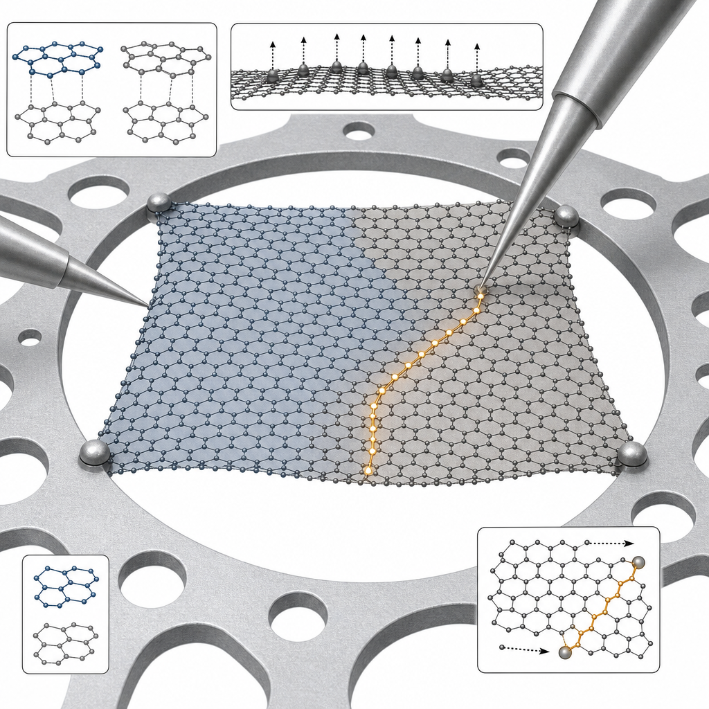
Key results include the first direct visualization of dislocation line tension as a restoring force: dislocations stretched to roughly three times their original length returned almost completely to their initial configuration upon tip release. The authors quantified how dislocation character changes from screw-type to edge-type along a single defect by tracking contrast width in tSEM, and validated their interpretation against the Burgers vector–line direction relationship. Three-fold dislocation nodes containing energetically unfavorable AA stacking were imaged at the meeting points of three partials with distinct Burgers vectors, in agreement with HRTEM analysis. Most strikingly, arrays of out-of-plane dislocations forming a small-angle tilt grain boundary (~0.2°) were shown to anchor pairs of in-plane partial dislocations of alternating screw and edge character. Using a fine tip, the team induced switching reactions in which in-plane dislocations recombined and rerouted between different out-of-plane anchor points, reconnecting separated AC-stacked regions into a continuous pathway while dividing the surrounding AB-stacked area. All defects carried Burgers vectors of type a/3⟨11-20⟩, and switching events were locally confined, leaving neighboring out-of-plane dislocations untouched.
These findings have direct implications for 2D-materials research, defect engineering, and the emerging field of topological electronics. The proposed dislocation-based topological switch — a bilayer graphene ribbon contacted at two ends with two out-of-plane dislocations as fixed anchors — could toggle between an "On" state with an open AB-stacking conduction path and an "Off" state where two parallel partial dislocations span the ribbon, potentially producing an insulating transport regime, especially under transverse magnetic fields. Beyond switches, the methodology enables systematic investigation of solitons, domain walls, plasmon reflection, and valley-polarized transport in van der Waals materials. Patterning techniques could translate the screened dislocation configurations shown in the paper into reproducible functional devices.
For researchers exploring dislocations, strain solitons, or stacking-domain engineering in 2D materials, this paper validates the use of ACS Material Trivial Transfer® Graphene as a reliable, transfer-ready bilayer film compatible with TEM grid mounting, PMMA removal, and free-standing in situ microscopy workflows. The product is available through the Trivial Transfer Series catalog for groups working on free-standing 2D membranes, defect dynamics, and topological device prototypes.How ACS Material products were used
- Trivial Transfer® Graphene (bilayer) (Trivial Transfer Series) — “Chemical vapor deposition–grown nominally bilayer graphene (Trivial Transfer Graphene) was purchased from ACS Material. The graphene films were delivered on a substrate and covered by a poly(methyl methacrylate) (PMMA) transfer layer.”
Product Performance in this StudyThe CVD-grown bilayer Trivial Transfer Graphene from ACS Material served as the free-standing membrane on which all in situ dislocation manipulation, imaging, and switching experiments were performed. The film transferred cleanly onto Quantifoil TEM grids and survived mechanical manipulation with tungsten micromanipulator tips, enabling high-resolution tSEM and HRTEM imaging of individual partial dislocations.
Related product categories
Frequently asked questionsWhy use free-standing CVD bilayer graphene to study dislocations?
Free-standing bilayer graphene is the thinnest crystalline solid known to host extended in-plane dislocations, and removing the substrate eliminates strong van der Waals interactions that would otherwise pin or distort defects. This lets researchers observe intrinsic line tension, screw/edge character transitions, and node formation directly, and apply mechanical force from both sides of the membrane using opposing micromanipulators.
How was the Trivial Transfer bilayer graphene mounted for in situ SEM manipulation?
The graphene was floated off its substrate on deionized water, cut into roughly 2 mm × 2 mm pieces, and picked up with Quantifoil TEM support grids. The PMMA protective layer was dissolved by 20 s of acetone immersion followed by 2 hours under saturated acetone vapor reflux, yielding clean free-standing bilayer membranes spanning the grid holes for transmission-mode SEM imaging.
What is a topological dislocation switch in bilayer graphene?
It is a proposed device in which two sessile out-of-plane dislocations act as fixed anchor points for mobile in-plane partial dislocations in a bilayer graphene ribbon. Mechanical manipulation toggles the partials between two configurations, opening or closing a continuous AB-stacked transport pathway. The two states are topologically distinct and may produce different electronic transport, especially under a transverse magnetic field.