-
Trivial Transfer Graphene Adhesion on Si - Beihang, 2017
Jul 09, 2026 | ACS MATERIAL LLCGao, X. et al. (2017). Measuring Graphene Adhesion on Silicon Substrate by Single and Dual Nanoparticle‐Loaded Blister. *Advanced Materials Interfaces*. https://doi.org/10.1002/admi.201601023
School of Instrumentation Science and Opto‐Electronics Engineering Beihang University Beijing 100191 China · Advanced Materials Interfaces · 2017
Beihang University researchers quantify CVD graphene adhesion on SiO2 using single and dual nanoparticle blister tests with Trivial Transfer Graphene.
About this research
Researchers at the School of Instrumentation Science and Opto-Electronics Engineering Beihang University Beijing 100191 China used Trivial Transfer Graphene supplied by ACS Material to develop an improved nanoparticle-loaded blister method for quantifying graphene-silicon interfacial adhesion, reporting adhesion energies of 0.453 J m-2, 0.317 J m-2, and 0.276 J m-2 for monolayer, 3-5 layer, and 10-15 layer films, respectively. Published in Advanced Materials Interfaces in 2017, the study introduces a generalized analytical model that handles both single- and dual-particle blisters, enabling more reliable data extraction from a single fabricated sample. The work bridges nanomechanics and 2D-materials metrology, providing a practical route to characterize membrane-substrate adhesion without specialized peel rigs or AFM nanoindentation.
Interfacial adhesion between graphene and its support substrate is a critical parameter for graphene-based nano-electromechanical sensors, pressure transducers, transparent electrodes, and stretchable electronics. Existing techniques such as AFM nanoindentation, double cantilever beam fracture tests, and inflated-gas blister tests each have drawbacks: thin sheets are easily damaged by clamps, AFM tip surface roughness must be modeled with corrections like the Rumpf approach, and pull-off instability disturbs tip-sample interactions. As graphene moves into industrial sensor packaging and flexible electronics, researchers need a simpler, equipment-light technique to map adhesion energy across substrates and layer thicknesses. The Beihang team addresses this gap with a nanoparticle blister geometry-only measurement that requires only SEM imaging.
The ACS Material Trivial Transfer Graphene was supplied as 10 mm x 10 mm CVD graphene grown on 20 um Cu foil and coated with a PMMA support on a polymer substrate, available in monolayer, 3-5 layer, and 10-15 layer grades. The team diced 500 um Si wafers with a 300 nm thermal SiO2 layer into 10 mm squares, ultrasonically cleaned them in acetone and alcohol, and dispersed 60 nm gold nanoparticles (BB International, 2.6 x 10^10 particles per mL) onto the substrate after centrifugation at 3000 rpm. The PMMA-supported graphene sheet was floated in deionized water, scooped onto the nanoparticle-decorated Si wafer, dried at 80 degrees C, and then the PMMA was etched in acetone. Van der Waals interaction between the graphene and SiO2 conformed the membrane around the trapped Au nanoparticles, forming circular blisters around isolated single particles and elliptical blisters around dual adjacent particles. AFM verified the SiO2 surface roughness was approximately 300 pm rms and confirmed multilayer thicknesses, e.g. 4.13 nm for the 10-15 layer film.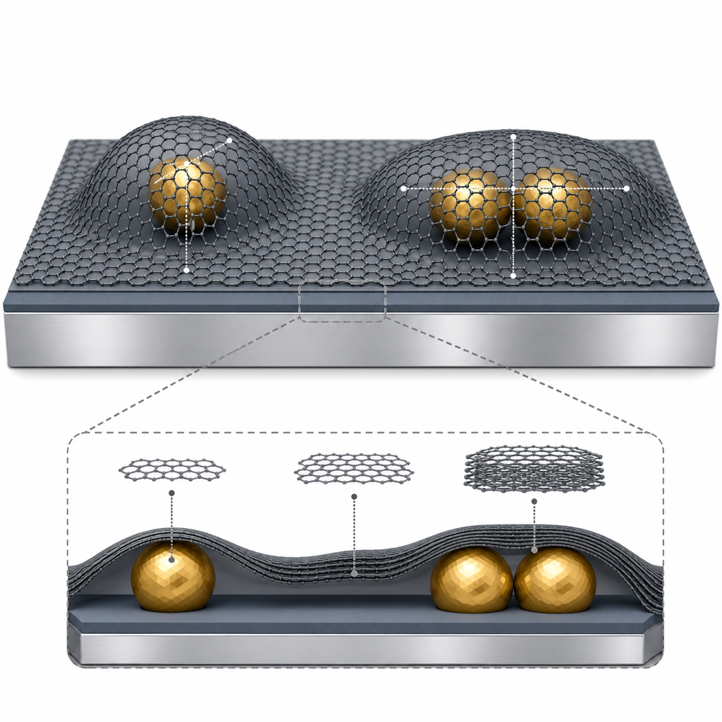
Using fracture mechanics for a shaft-loaded membrane, the team derived a unified governing relation Gamma = E t (h/a)^4 / C, with C = 16 for single-particle circular blisters and C = 64 for dual-particle elliptical blisters when the semiminor axis is used as the equivalent debonding radius. SEM imaging on the JSM-7500F provided the blister radii: 156, 242, and 336 nm for single-particle circular blisters on monolayer, 3-5 layer, and 10-15 layer membranes, and corresponding semiminor axes of 111, 171, and 237 nm for dual-particle elliptical blisters - precisely the a/sqrt(2) scaling predicted by the dual-particle model. Taking E = 1 TPa, the extracted adhesion energies were 0.453 +/- 0.006 J m-2 (monolayer), 0.317 +/- 0.003 J m-2 (3-5 layer), and 0.276 +/- 0.002 J m-2 (10-15 layer), under a 3 sigma criterion. Results from the dual-particle and single-particle analyses deviated by at most 1.6 percent. The monolayer value matches the 0.46 J m-2 reported by Jiang and Zhu via AFM, the 3-5 layer value matches Koenig et al.'s 0.31 J m-2, and the 13-layer result coincides with theoretical predictions of 0.277 J m-2 and a previously measured 0.275 J m-2 at the graphene-ZrO2 interface, validating the method.
The nanoparticle blister approach is directly relevant to graphene pressure sensors, NEMS resonators, gas-impermeable membranes, optical fiber Fabry-Perot devices, and any flexible electronic application where peeling or delamination determines device lifetime. Because the analysis is geometry-based, the technique extends to other 2D materials such as hexagonal boron nitride, MoS2, and WSe2 on arbitrary substrates including silicon dioxide, quartz, ZrO2, and polymer films. The authors propose future work on multiple-nanoparticle configurations and substrate deformation effects, which could refine traction-separation models used in finite-element simulations of 2D-material/dielectric stacks. For sensor manufacturers, the method offers a low-cost quality-control inspection that requires only SEM access.
For researchers reproducing or extending this work, ACS Material supplies the same CVD Trivial Transfer Graphene used here in monolayer through multilayer grades, along with complementary 2D materials such as Trivial Transfer h-BN, CVD graphene on copper foil, and exfoliated transition metal dichalcogenides. The consistent layer quality and PMMA-supported transfer process described in the paper make this product line a practical starting point for adhesion, NEMS, and flexible electronics studies that need reproducible 2D films delivered ready for transfer onto user substrates.How ACS Material products were used
- Trivial Transfer® Graphene (monolayer, 3-5 layer, and 10-15 layer) (Trivial Transfer Series) — “The graphene membrane (monolayer, 3–5 layer and 10–15 layer), with a 10 mm × 10 mm area, was prepared from a commercial trivial transfer graphene sheet in which it was grown by CVD on a 20 µm thick Cu foil deposited on a polymer substrate (ACS Material, www.xfnano.com).”
Product Performance in this Study
The CVD-grown Trivial Transfer graphene served as the central test material. Its clean PMMA-supported transfer onto SiO2/Si substrates enabled formation of well-defined circular and elliptical blisters around intercalated gold nanoparticles, yielding repeatable adhesion energies of 0.453, 0.317, and 0.276 J m-2 for monolayer, 3-5 layer, and 10-15 layer films, in excellent agreement with literature values.
Related product categories
Frequently asked questions
How does the nanoparticle blister test measure graphene adhesion energy?
A flat 2D membrane is draped over a substrate decorated with nanoparticles, trapping each particle inside a small blister. By measuring the blister diameter and height with SEM and applying a fracture-mechanics model Gamma = E t (h/a)^4 / C, the interfacial adhesion energy is extracted. Geometry alone provides the data, so no pressurized gas chamber or AFM nanoindenter is required.
What adhesion energies were obtained for graphene on SiO2 in this study?
Using Trivial Transfer CVD graphene from ACS Material, the team measured 0.453 J m-2 for monolayer, 0.317 J m-2 for 3-5 layer, and 0.276 J m-2 for 10-15 layer graphene on a 300 nm SiO2/Si substrate. These values agree with prior AFM and pressurized blister measurements to within a few percent, and the 13-layer result matches a theoretical graphene-SiO2 adhesion energy of 0.277 J m-2.
Why does graphene adhesion energy decrease with increasing layer number?
Adhesion at a 2D-material/substrate interface is governed by short-range van der Waals interactions and how well the membrane conforms to the substrate's roughness. Thicker multilayer graphene has higher bending rigidity, so it cannot wrap as closely around surface asperities. With less intimate contact, the effective adhesion energy drops from about 0.45 J m-2 for monolayers to about 0.28 J m-2 for 10-15 layer films.