-
Trivial Transfer Graphene for 2D Heterostructures - FU Berlin, 2025
Jun 03, 2026 | ACS MATERIAL LLCChen, X. et al. (2025). Patterned Assembly of Transition Metal Dichalcogenide/Graphene Heterostructures via Direct Laser Writing. *Advanced Functional Materials*. https://doi.org/10.1002/adfm.202425776
Institute of Chemistry and Biochemistry Freie Universität Berlin Altensteinstraße 23a 14195 Berlin Germany · Advanced Functional Materials · 2025
Researchers at Freie Universität Berlin used ACS Material Trivial Transfer graphene to build laser-written TMD/graphene heterostructures via direct laser writing.
About this research
Researchers at Freie Universität Berlin, working with collaborators at Friedrich-Alexander-Universität Erlangen-Nürnberg, used ACS Material's Trivial Transfer monolayer graphene as the bottom substrate to demonstrate a direct laser writing method that assembles and patterns covalently linked transition metal dichalcogenide (TMD)/graphene heterostructures in a single run. Functionalized TMD nanosheets (MoS2, WS2, MoSe2) bearing photolabile iodophenyl groups were deposited as inks on the graphene film, and a focused 532 nm Raman laser selectively triggered localized photochemical reactions, forming chemically modified domains only in irradiated regions. This conceptual parallel to laser printing replaces costly lithography with a mask-free, reproducible approach for fabricating spatially defined 2D heterostructures.
Vertically stacking different 2D layers into heterostructures is a powerful strategy to engineer electronic, optical, and catalytic properties, but conventional assembly via mechanical stacking, epitaxial growth, or CVD relies on expensive instrumentation and delicate condition control. Even when molecular crosslinkers are used to covalently connect 2D building blocks, the random accumulation of flakes compromises homogeneity and complicates subsequent patterning. The open challenge is achieving high-throughput, customizable, and patternable heterostructure assembly that remains compatible with downstream device integration. This work addresses that gap by combining solution-processed, functionalized 2D inks with photolabile linkers and laser-induced coupling, enabling programmable interface chemistry that is directly relevant to flexible electronics, sensors, and optoelectronic devices.
The ACS Material Trivial Transfer graphene was the foundational layer of every heterostructure. The monolayer graphene, supplied as a 10 mm × 10 mm film covered by a PMMA support, was floated onto the surface of water and fished onto a Si/SiO2 wafer. The graphene-on-substrate was dried at room temperature and at 100 °C to remove water, then immersed in preheated acetone (50 °C) to dissolve the PMMA, leaving a clean graphene film. Pre-assembled functionalized TMD layers, formed at a toluene–water interface by a modified Langmuir–Blodgett method, were then transferred on top of the graphene to create fun-TMD/graphene stacks. The graphene therefore acted both as the chemical reaction partner for photogenerated phenyl radicals and as the readout layer for Raman mapping. Its lattice quality was central: the inverse relationship between the graphene I(2D)/I(G) ratio and defect density provided the principal experimental signature of covalent interface coupling, making the quality and uniformity of the transferred graphene essential to the entire patterning workflow.
The study produced several quantitative findings. Raman mapping with a 1 μm step over 5 × 5 μm² areas used a high writing laser power of 12–17 mW (12 mW for fun-MoS2/G, 15 mW for fun-WS2/G, 17 mW for fun-MoSe2/G) and a 2 or 7 mW reading power. Increasing laser power lowered the graphene I(2D)/I(G) ratio, raising defect density until saturation at about 10 mW, indicating an initially energy-limited and then reactant-limited reaction. The I(G)/I(2D) ratio rose from 0.5 to 3.5 as interactions strengthened. At 23.1 mW, functional-group peaks in the 1300–1600 cm⁻¹ range disappeared, signaling de-functionalization. KPFM on a 10 × 10 μm² written pattern showed a maximum surface potential difference of ≈0.24 V between irradiated and non-irradiated regions. XPS confirmed deiodination: iodine 3d5/2 and 3d3/2 peaks at 619.3 and 630.8 eV present in non-irradiated regions vanished after irradiation, while the C–OH component of the C 1s spectrum increased. ToF-SIMS over domains up to 300 × 300 μm² mapped elevated O⁻ and OH⁻ signals in irradiated regions, consistent with MoOx formation and phenol generation. DFT calculations gave reaction energies of −1.7 eV (biphenyl pathway) and −3.7 eV (phenol pathway), with average interlayer Mo–Mo distances of 14.1, 14.8, and 9.7 Å for the biphenyl, phenol, and phenyl motifs, supporting the proposed covalent coupling chemistry. The functionalization degree was measured at 33 ± 1%.
This laser-writing strategy enables high-throughput, mask-free fabrication of customizable 2D heterostructures, lowering both cost and time relative to electron-beam lithography. Because the functionalized TMD inks can be extended to other solution-processable 2D materials, the method offers a programmable route to printing functional heterostructures for flexible electronics, sensors, and optoelectronics. The authors highlight the ability to spatially tune interlamellar gaps and interface chemistry through laser-triggered reactions, opening a path toward mass production of heterostructure-based devices and novel 2D/3D nanoarchitectures. Follow-up work pointed to by the paper includes exploiting photolabile linkers and photoinduced coupling for more complex multilayer patterning and integrating the inks with advanced deposition techniques.
For researchers pursuing similar 2D heterostructure assembly, the reliability of the bottom graphene layer is decisive, since the covalent coupling signature is read directly from the graphene Raman response. ACS Material's Trivial Transfer graphene, the PMMA-supported monolayer film used here, is available for groups working on covalent 2D functionalization, laser-patterned interfaces, and printed heterostructure devices. The product served its role as a clean, transferable graphene substrate, and the paper's results illustrate the kind of interface chemistry and patterning studies it supports.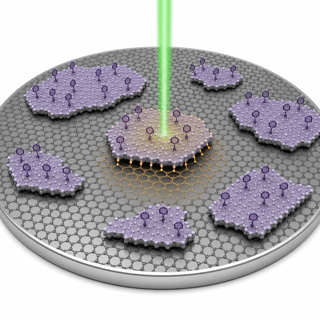
How ACS Material products were used
- Trivial Transfer® Graphene (monolayer, PMMA-coated, 10 mm × 10 mm) (Trivial Transfer Series) — “Monolayer trivial transfer G (10 mm × 10 mm) covered by poly (methyl methacrylate) (PMMA) was purchased from ACS material.”
Product Performance in this Study
The CVD-grown monolayer graphene served as the bottom layer onto which functionalized TMD inks were deposited and patterned. It enabled covalent interface coupling, and Raman/KPFM confirmed laser-induced functionalization of the graphene lattice.
Related product categories
Frequently asked questions
What is Trivial Transfer graphene used for in 2D heterostructure fabrication?
Trivial Transfer graphene serves as a transferable monolayer bottom layer that can be floated onto water and placed on target substrates such as Si/SiO2. In this study it acted as both the covalent reaction partner for photogenerated phenyl radicals from functionalized TMD inks and the readout layer for Raman mapping, enabling laser-written, patterned TMD/graphene heterostructures.
How does laser power affect covalent coupling between functionalized MoS2 and graphene?
Higher 532 nm Raman laser power lowers the graphene I(2D)/I(G) ratio, increasing defect density from covalent bonding of photogenerated phenyl radicals to graphene. Defect formation rises until saturation near 10 mW, then plateaus. Around 12 mW gives strong functionalization, while 23.1 mW removes functional groups entirely, indicating de-functionalization at very high power.
Why is graphene quality important for laser-written heterostructure patterning?
The covalent coupling signal is read directly from the graphene lattice via the Raman I(2D)/I(G) ratio, which is inversely related to defect density. A clean, uniform monolayer is therefore essential so that laser-induced changes reflect genuine interface chemistry rather than pre-existing defects, allowing accurate mapping of patterned, chemically modified domains.