-
Trivial Transfer Graphene for Atomic HRTEM - FAU Erlangen, 2022
Jun 09, 2026 | ACS MATERIAL LLCDolle, C. et al. (2022). Atomically resolved TEM imaging of covalently functionalised graphene. *npj 2D Materials and Applications*. https://doi.org/10.1038/s41699-022-00304-w
npj 2D Materials and Applications · 2022
Researchers at FAU Erlangen used ACS Material Trivial Transfer Graphene to image covalently functionalized monolayer graphene at atomic resolution by HRTEM.
About this research
Researchers at Friedrich-Alexander-Universität Erlangen-Nürnberg, together with collaborators at the Universidad de Valencia, used PMMA-coated Trivial Transfer Graphene supplied by ACS Material to demonstrate the first atomically resolved transmission electron microscopy (TEM) images of wet-chemically, covalently functionalized monolayer graphene. The team reductively alkylated suspended graphene membranes with dodecyl iodide, removed physisorbed contamination using an in situ mechanical gold-tip cleaning approach, and resolved individual covalently bound dodecyl addends on the graphene basal plane. The result is published in npj 2D Materials and Applications (2022) and provides the missing direct microscopic verification of a chemistry that was previously documented mostly by Raman and other ensemble methods.
Covalent functionalization is one of the most powerful tools for tuning graphene's electronic, optical, and chemical behavior. Introducing isolated sp³ defects can open a bandgap, generate binding sites for biomolecular probes, and induce localized magnetic moments. Yet despite the maturity of wet-chemical functionalization protocols, the field has lacked direct atomic-scale images of the resulting hybrid materials because residual solvents and physisorbed hydrocarbons systematically obscure HRTEM contrast. Closing this gap matters for everyone working on graphene-based sensors, optoelectronic devices, spintronic platforms, and protein-nanomaterial interfaces, because the spatial homogeneity and exact bonding geometry of addends ultimately controls device performance.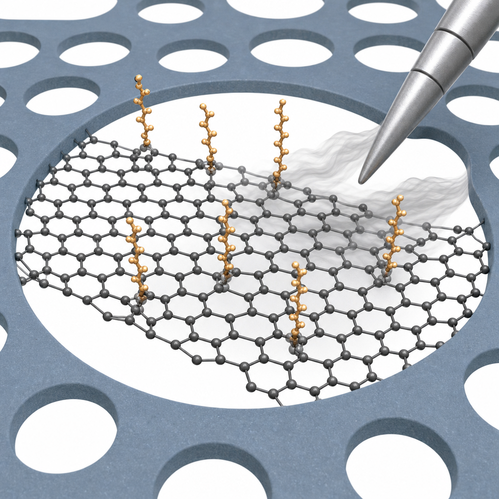
The ACS Material Trivial Transfer Graphene product was central to the workflow. The team received CVD monolayer graphene on a hydrophobic support coated with PMMA, infiltrated the support with water, floated the PMMA/graphene film, cut it into roughly 2 × 2 mm² pieces, and re-floated and fished the flakes onto pre-cleaned Quantifoil TEM grids with nominal 2 µm hole diameter. The grids were dried at 100 °C for 10 min to promote adhesion, and PMMA was dissolved in acetone followed by 2 h of acetone vapor reflux. The freestanding monolayer was then carried into an argon glove box (<0.1 ppm O₂/H₂O) and chemically activated with 30 µL of a Na/K eutectic alloy dissolved in absolute DME, after which 30 µL of dodecyl iodide was added. The reaction was quenched after 15 min by rinsing with DME. Because the graphene was already suspended on the TEM grid, it could be moved directly from synthesis to imaging without an additional transfer step that would have introduced new contamination.
The imaging results validate the methodology with quantitative depth. Raman spectra on the TEM grid before and after reaction showed a strong increase in the D band at 1350 cm⁻¹ and the appearance of D' at 1622 cm⁻¹ and D + D' at 2930 cm⁻¹, confirming sp²-to-sp³ rehybridization. DFT calculations gave a C–C cleavage energy of 1.55 eV for a (1,2)-anti dodecyl/H pair, ruling out merely radical or ionic stabilization. After mechanical filtering with a gold double-tip, atomically clean regions of about 5 µm² were obtained. Aberration-corrected HRTEM at 80 kV (Cs ≈ −10 µm, 200 meV energy spread, 500 ms exposure) revealed localized, spot-like contrast features in the graphene lattice corresponding to dodecyl attachment sites. A novel simulation pipeline that fed up to 30,000 frames of 50 ns classical MD trajectories into Kirkland multislice HRTEM simulations reproduced the experimental contrasts across multiple defocus values. Area coverage was estimated at 0.06%, consistent with the ~0.1% degree of functionalization reported for comparable systems and with the mean defect spacing of ~7 nm implied by the measured I_D/I_G ratio of 2.3. The hybrid material withstood accumulated electron doses up to 5 C cm⁻² before defunctionalization, during which time the team observed five sequential molecular jumps of one addend in a roughly clockwise migration pattern.
The study opens the way to atomic-resolution structural studies of any wet-chemically functionalized 2D material, not just graphene. Practically, it means that researchers developing covalent chemistries for bandgap engineering, biosensor functionalization, magnetic graphene, energy storage electrodes, and 2D heterostructure assembly can now correlate spatial homogeneity, defect density, and bonding motif directly with single-molecule images. The combined MD-plus-HRTEM image simulation framework is also generalizable: it should support imaging studies of functionalized hexagonal boron nitride, transition-metal dichalcogenides, and graphdiyne, where thermally driven addend motion otherwise blurs HRTEM contrast.
For researchers planning similar work, the lesson is that starting-material quality determines what can be imaged. Clean, well-supported, freestanding CVD monolayer graphene with a reliable transfer process is a prerequisite. The Trivial Transfer Graphene used in this study is available through ACS Material for groups building functionalized graphene devices, 2D heterostructures, and TEM-based chemistry experiments who need a reproducible PMMA-supported CVD graphene starting platform.How ACS Material products were used
- Trivial Transfer® Graphene (PMMA-coated CVD monolayer graphene) (Trivial Transfer Series) — “Freestanding monolayer graphene samples on Quantifoil grids were prepared from PMMA coated Trivial Transfer Graphene supplied by ACS Materials.”
Product Performance in this StudyThe PMMA-coated Trivial Transfer Graphene from ACS Material served as the freestanding monolayer graphene starting platform for covalent dodecyl functionalization and atomic-resolution HRTEM imaging. Its clean, transferable monolayer character was essential to producing suspended membranes on Quantifoil grids that survived wet-chemical reductive alkylation and in situ mechanical cleaning.
Related product categories
Frequently asked questionsWhy is PMMA-coated CVD graphene used as the starting material for covalent functionalization studies?
PMMA-coated CVD monolayer graphene can be released from its growth substrate by water infiltration and floated onto TEM grids, producing freestanding suspended membranes with large clean areas. The PMMA layer mechanically protects the graphene during transfer and is removed by acetone wash. This workflow gives reproducible, atomically thin starting samples suitable for both wet-chemical reactions and high-resolution electron microscopy without an extra transfer step.
How does mechanical filtering enable atomic-resolution TEM of functionalized graphene?
Wet-chemical functionalization leaves physisorbed hydrocarbons that obscure HRTEM contrast. By sweeping a fine gold tip across both faces of the freestanding membrane inside the TEM, contaminants held by ~40 meV cohesive bonds are removed, while covalent C–C bonds (~1 eV or more) to dodecyl addends remain intact. The selectivity converts cleaning into filtering, exposing atomically clean regions of about 5 µm² for imaging.
What is the typical degree of functionalization observed for dodecyl-graphene hybrids?
In this study, HRTEM image analysis gave a dodecyl area coverage of about 0.06%, consistent with the roughly 0.1% degree of functionalization reported for comparable reductive alkylation systems. The Raman I_D/I_G ratio of about 2.3 corresponds to a mean defect spacing near 7 nm. These values indicate that the addends are isolated, dilute sp³ sites rather than continuous coverage, which is desirable for bandgap and magnetic property tuning.