-
Trivial Transfer Graphene for Laser Patterning - FAU Erlangen-Nürnberg, 2025
Jun 03, 2026 | ACS MATERIAL LLCNagel, T. et al. (2025). Towards precision controlled 2D functional group patterning of graphene via laser writing. *Carbon*. https://doi.org/10.1016/j.carbon.2025.120376
Carbon · 2025
FAU Erlangen-Nürnberg used ACS Material Trivial Transfer Graphene for laser-triggered covalent functional-group patterning, reaching 1.5 µm and 300 nm features.
About this research
Researchers at Friedrich-Alexander-Universität Erlangen-Nürnberg (FAU) used ACS Material Trivial Transfer Graphene (CVD monolayer graphene supplied with a PMMA coating) to demonstrate a high-precision, laser-triggered approach for covalently patterning functional groups onto monolayer graphene, achieving controlled feature sizes down to 1.5 µm and as small as 300 nm when combined with a lithographic mask. The work, published in Carbon (2025), clarifies the mechanism of laser-activated dibenzoyl peroxide (DBPO) grafting and shows how laser power and irradiation time govern the degree of functionalization. A key methodological advance is the full deconvolution of the laser "writing" step from the Raman "reading" step by completely removing the reactive DBPO film after grafting.
This research matters because spatially resolved chemical modification of graphene allows local tailoring of conductivity, doping, and addend coverage—essential for building functional 2D devices and for chemical information storage. Existing patterning routes rely on costly, complex pre-structuring: either exploiting substrate-dependent reactivity or coating graphene with PMMA followed by lithographic masking before classical functionalization. These approaches share a sophisticated pre-patterning bottleneck. Direct laser writing offers a simpler alternative by using a locally controlled activation source to trigger covalent chemistry only where needed. However, prior laser-writing methods could not remove the reactive precursor film after grafting, so the Raman readout laser caused unwanted secondary functionalization. The field needed a clean separation of writing and reading to truly understand and control the chemistry, which this paper provides.
The ACS Material Trivial Transfer Graphene was the central material. The CVD monolayer graphene, delivered with a PMMA support layer, was wet-transferred onto Si/SiO2 wafers (300 nm oxide) using an optimized transfer technique. A DBPO film was then spin-coated onto the graphene from a 10⁻³ M diethyl ether solution (1–2 drops, 4000 rpm) to form a uniform reactive layer. The sample was irradiated in a Raman spectrometer using a 532 nm green laser in a line-based scanning mode, attaching phenyl groups while monitoring functionalization in situ. After writing, the sample was removed and the residual DBPO coating was washed off by immersion in diethyl ether for 10 minutes, rinsing with isopropanol, and drying under pressurized air, preventing unwanted modification during the Raman readout. As stated in the Materials section, "CVD graphene was purchased from ACS Materials Inc. as trivial transfer graphene with PMMA coating." The graphene's pristine sp² lattice—confirmed by a strong G band near 1582 cm⁻¹ and negligible D band—provided the clean baseline needed to quantify grafting.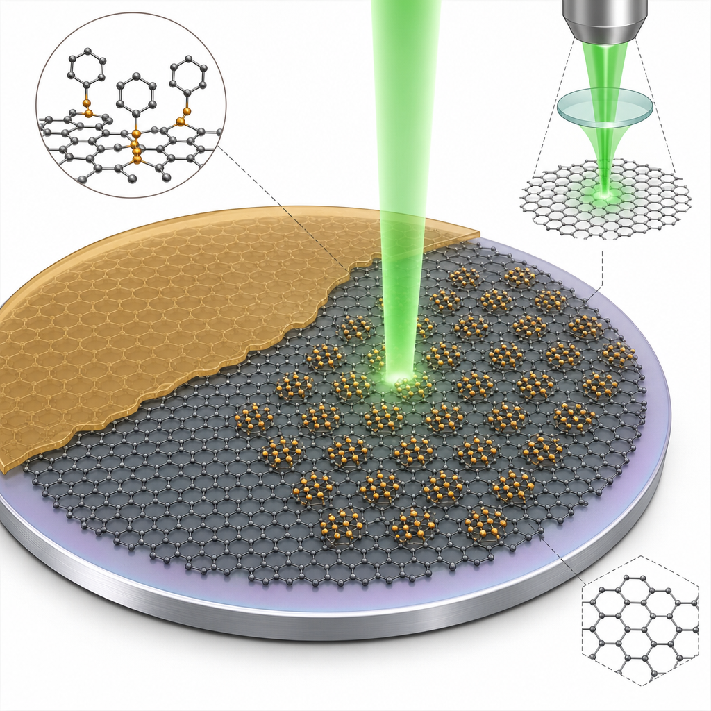
The key results quantify how laser parameters control covalent attachment. After laser writing, a pronounced D band appeared, indicating conversion of sp² to sp³ carbon from phenyl radical binding. The team demonstrated that increasing laser power raised the degree of functionalization up to a maximum, then decreased above 10 mW; between 0.5 and 10 mW the irradiation time was the dominant lever, with D band intensity peaking at 2 s exposure. Mechanistic analysis—supported by DFT—ruled out direct photoexcitation (DBPO shows no visible absorption) and thermal decomposition, instead favoring hot-electron transfer from laser-excited graphene to the DBPO LUMO (ΔE ≈ 1.6 eV; HOMO at −2.3 eV). Functionalization succeeded under blue (457 nm), green (532 nm), and red (633 nm) excitation, consistent with the hot-electron model. Thermal deactivation of the DBPO film was achieved fully at 75 °C for 30 min (partial at 50 °C). With optimized parameters (0.5 mW), the smallest resolvable pattern separation reached 1.5 µm with a 1.5 µm feature diameter; combining electron-beam-lithography PMMA masks (lines of 2, 1, 0.5, and 0.3 µm) with laser writing produced well-resolved 300 nm features below the diffraction limit. The covalently bound phenyl moieties showed long-term stability exceeding 13 months and thermal stability up to 125 °C.
These capabilities enable functional graphene-based devices, reversible chemical information storage and processing, and tailored 2D heterostructures where local conductivity and doping must be defined with sub-micron precision. The paper notes the concept can be extended to other photolabile compound classes—benzoyl peroxides, hypervalent iodine reagents, perfluorinated polymers, and silver carboxylates—broadening the chemistry toolkit. Because writing and reading are now cleanly decoupled, researchers can reproducibly fine-tune functionalization for applications in flexible electronics, sensing, and patterned 2D materials. The combination with lithographic masks points toward nanoscale chemical patterning suitable for next-generation device fabrication and rewritable molecular memory on graphene.
For researchers pursuing similar 2D-functionalization, sensing, or device work, the monolayer CVD graphene used here is the Trivial Transfer Graphene product line offered by ACS Material, available with PMMA support for clean wet transfer onto arbitrary substrates. The paper's results confirm the material provided a reliable, low-defect monolayer baseline that made quantitative Raman-monitored covalent patterning possible. This consistency is what makes the product useful as a starting platform for laser-writing chemistry and other precision graphene modification studies.How ACS Material products were used
- Trivial Transfer® Graphene (CVD monolayer graphene with PMMA coating) (Trivial Transfer Series) — “CVD graphene was purchased from ACS Materials Inc. as trivial transfer graphene with PMMA coating.”
Product Performance in this StudyThe Trivial Transfer Graphene served as the monolayer graphene substrate that was wet-transferred onto Si/SiO2 and covalently patterned by laser writing. Its quality enabled reproducible Raman-monitored functionalization down to 1.5 µm (0.3 µm with a mask).
Related product categories
Frequently asked questionsWhat graphene was used for laser-triggered covalent patterning in this study?
The study used CVD monolayer graphene purchased from ACS Material as Trivial Transfer Graphene with a PMMA coating. It was wet-transferred onto Si/SiO2 wafers with a 300 nm oxide layer, then coated with dibenzoyl peroxide and patterned by laser writing. The pristine sp² lattice provided the clean baseline needed to quantify covalent phenyl-group attachment by Raman spectroscopy.
How do laser power and irradiation time control graphene functionalization?
Increasing laser power raised the degree of functionalization to a maximum, then decreased above 10 mW. Between 0.5 and 10 mW, irradiation time dominated, with the D band intensity peaking at 2 seconds of exposure. Adjusting these two parameters lets researchers fine-tune the density of covalently bound phenyl groups while balancing degree of functionalization against lateral patterning precision.
What is the smallest pattern size achievable with laser writing on graphene?
Using optimized 0.5 mW writing parameters, the smallest resolvable pattern separation and feature diameter were both about 1.5 µm. Combining the laser-writing approach with an electron-beam-lithography PMMA mask reduced features to 300 nm, below the diffraction limit of visible light, while still allowing precise control of the degree of covalent functionalization.