-
Trivial Transfer Graphene for Self-Heating Devices - Sandia, 2016
Jul 07, 2026 | ACS MATERIAL LLCBeechem, T. E. et al. (2016). Self-heating and failure in scalable graphene devices. *Scientific Reports*. https://doi.org/10.1038/srep26457
Scientific Reports · 2016
Sandia researchers used ACS Material Trivial Transfer graphene to build CVD graphene devices that dissipate >3x the power of epitaxial graphene before failure.
About this research
Sandia National Laboratories researchers used ACS Material Trivial Transfer® Graphene to fabricate CVD graphene devices on 6H-SiC substrates and compared their self-heating behavior with epitaxially grown graphene, finding that the CVD devices dissipate more than three times the power before failure than their epitaxial counterparts. Combining infrared thermography and Raman thermal imaging, the team mapped local temperature distributions during electrical operation and correlated hot spots with morphological features identified by the Raman 2D-mode peak position. The conclusion is counterintuitive: morphology, not interfacial thermal resistance, dictates the power-handling limit of large-area graphene devices.
Scalable graphene is essential for any practical microelectronic or optoelectronic application, but the very synthesis routes that deliver wafer-area material — CVD on copper followed by transfer, or sublimation-grown epitaxial graphene on SiC — also introduce defects, wrinkles, multilayer patches, and transfer debris. These features cause non-uniform carrier concentration and non-uniform resistance, which in turn localize Joule heating. Existing self-heating studies on exfoliated graphene have shown that heat is generated unevenly and that cross-plane heat coupling into the substrate, rather than in-plane conductivity of graphene itself, dominates thermal management. This paper extends those insights to the scalable, device-relevant forms of graphene that are actually available commercially, which makes the findings directly useful to anyone building real circuits.
The CVD graphene used in the devices was ACS Material Trivial Transfer® Graphene, transferred onto 6H-SiC substrates following the vendor's procedure. Conventional photolithography defined channels in four sizes — 5×15, 10×30, 15×45 and 20×60 μm — with metal contacts patterned to match the epitaxial graphene control devices. For dielectric-covered (Cov) variants, a thin Al2O3 buffer was first formed by controlled oxidation of an e-beam-evaporated Al layer, followed by 50 nm of HfO2 grown by ALD (Picosun Sunale R150, TDMAH and H2O precursors at 250 °C). For the epitaxial counterparts, quasi-free-standing monolayer graphene was synthesized on SiC and covered with 50 nm PECVD SiO2. This parallel device geometry isolates the graphene synthesis pathway as the principal experimental variable. Thermal imaging used a Quantum Focus Instruments InSb-based IR camera with ~2 μm lateral resolution; Raman maps were acquired with a WiTec Alpha300R at 532 nm and ~350 nm spot size, with 225 nm pixel spacing.
At comparable bias, CVD devices on SiC reached failure at power densities exceeding 57 mW/μm in the best cases, more than three times the failure threshold of epitaxial graphene on the same SiC substrate. The IR images show that uniformly transferred CVD regions produced an even temperature field even at ~515 mW total dissipation, whereas devices containing multilayer patches developed pronounced local hot spots and failed at only ~21 mW/μm. Post-failure Raman maps of the 2D-mode peak position overlap precisely with the hottest regions seen in the IR maps, demonstrating that morphological inhomogeneities — multilayer islands, wrinkles, transfer residues — concentrate current and heat until catastrophic breakdown occurs. This outcome runs against the expectation from thermal resistance alone: SiC has roughly three times the thermal conductivity of Si, and epitaxial graphene avoids the van der Waals Kapitza resistance at the graphene/substrate interface, so on a purely thermal basis the epitaxial devices should outperform CVD devices. Instead the morphological uniformity of the transferred CVD film wins.
The practical implication is that engineers designing high-power graphene transistors, RF amplifiers, transparent electrodes, photodetectors and interconnects should treat film uniformity as a first-order figure of merit, not a secondary cosmetic concern. Quality control by Raman 2D-mode mapping prior to device operation can predict failure-prone regions. The findings also suggest that improvements in CVD synthesis and transfer cleanliness translate directly into higher power-handling capacity, which is encouraging for the roll-to-roll graphene supply chain. Possible follow-up directions noted by the field include refined transfer chemistries, polymer-free transfer, larger single-crystal CVD domains and engineered interfaces that combine the morphological uniformity of CVD with the thermal advantages of direct SiC growth.
For researchers working on graphene electronics, thermal management, or any application where Joule heating limits device lifetime, the ACS Material Trivial Transfer® Graphene used in this study is available for similar device-fabrication work, along with related CVD graphene-on-copper, graphene-on-SiO2, and graphene-on-quartz products. The paper's central message — that material morphology controls failure — gives a clear quality criterion for selecting and inspecting graphene for power-handling applications, and supports the use of well-characterized commercial transfer films as a reliable starting point for scalable device studies.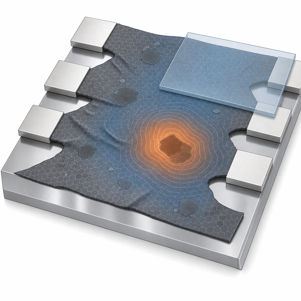
How ACS Material products were used
- Trivial Transfer® Graphene (Trivial Transfer Series) — “Analogous CVD devices were fabricated by transferring ACS 'Trivial Transfer' graphene onto 6H-SiC substrates using a procedure specified by the vendor.”
Product Performance in this Study
ACS Material's Trivial Transfer graphene served as the CVD graphene channel in the comparison devices. These CVD/SiC devices dissipated more than three times the power before failure than the epitaxial graphene counterparts, demonstrating that the transferred CVD graphene supplied by ACS enabled high-power operation despite its larger thermal interface resistance.
Related product categories
Frequently asked questions
Why do CVD graphene devices outperform epitaxial graphene devices in power handling?
In this Sandia study, CVD graphene devices on SiC dissipated more than three times the power before failure compared with epitaxial graphene on the same substrate. Although the CVD/SiC interface has higher van der Waals thermal resistance, the transferred CVD film was more morphologically uniform, while the epitaxial film contained multilayer patches that localized current and heat. Morphology, not thermal resistance, dictated the failure threshold.
How is Raman 2D-mode mapping used to predict graphene device failure?
Raman 2D-mode peak position is sensitive to layer number, strain, and doping. The authors mapped the 2D mode before electrical stressing and found that regions with non-uniform peak position correlated with hot spots in subsequent infrared thermography and with the locations where the device eventually broke down. Pre-operation Raman maps therefore serve as a non-destructive predictor of failure-prone regions in transferred CVD graphene.
What substrate effects matter most for self-heating in scalable graphene devices?
Heat dissipation in graphene devices is dominated by cross-plane coupling into the substrate rather than by graphene's own in-plane thermal conductivity. SiC offers about three times the thermal conductivity of silicon and avoids an insulating SiO2 layer when graphene is grown epitaxially. However, the study shows that even on high-conductivity SiC, morphological inhomogeneities in the graphene itself can localize heating and trigger early failure.