-
Trivial Transfer Graphene for TEM Defect Analysis - NIMS, 2026
Jun 26, 2026 | ACS MATERIAL LLCEguchi, R., & Hashimoto, A. (2026). Multiscale structural analysis of defective graphene in transmission electron microscopy images using persistent homology. *APL Materials*. https://doi.org/10.1063/5.0305461
National Institute for Materials Science 1 , 1-2-1 Sengen, Tsukuba, Ibaraki 305-0047, · APL Materials · 2026
NIMS researchers used ACS Material Trivial Transfer Graphene to develop a persistent-homology framework that quantifies multiscale defects in HR-TEM images of graphene.
About this research
Researchers at the National Institute for Materials Science used ACS Material Trivial Transfer Graphene as the single-layer specimen to develop a persistent-homology (PH) framework that converts transmission electron microscopy images of defective graphene into quantitative, multiscale structural descriptors. The transferred graphene was imaged by aberration-corrected HR-TEM, and the PH pipeline extracted both local carbon-atom polygon geometry and the global connectivity between rings. The headline result is an automated, label-free method that identifies defect types, measures ring distortion (roundness) and polygon number, and quantifies how electron-beam irradiation drives interconnected growth of defect clusters - all without the large annotated datasets that conventional deep-learning segmentation requires.
Understanding disordered structure-property relationships is central to studies of glassy and amorphous materials, and graphene is an ideal 2D testbed because TEM can directly visualize its atomic arrangement. Ideal graphene is a perfect lattice of six-membered carbon rings, but lattice defects are ubiquitous and they reshape electronic transport and magnetic behavior. Existing characterization has been largely confined to ring-size distributions, while the spatial distribution and nanometer-scale connectivity of carbon rings - degrees of freedom that govern emergent properties such as metallic line defects - have remained underexplored. This work addresses that gap with a multiscale topological descriptor, relevant to defect engineering for thermoelectrics, spintronics, and the modeling of amorphous 2D carbon.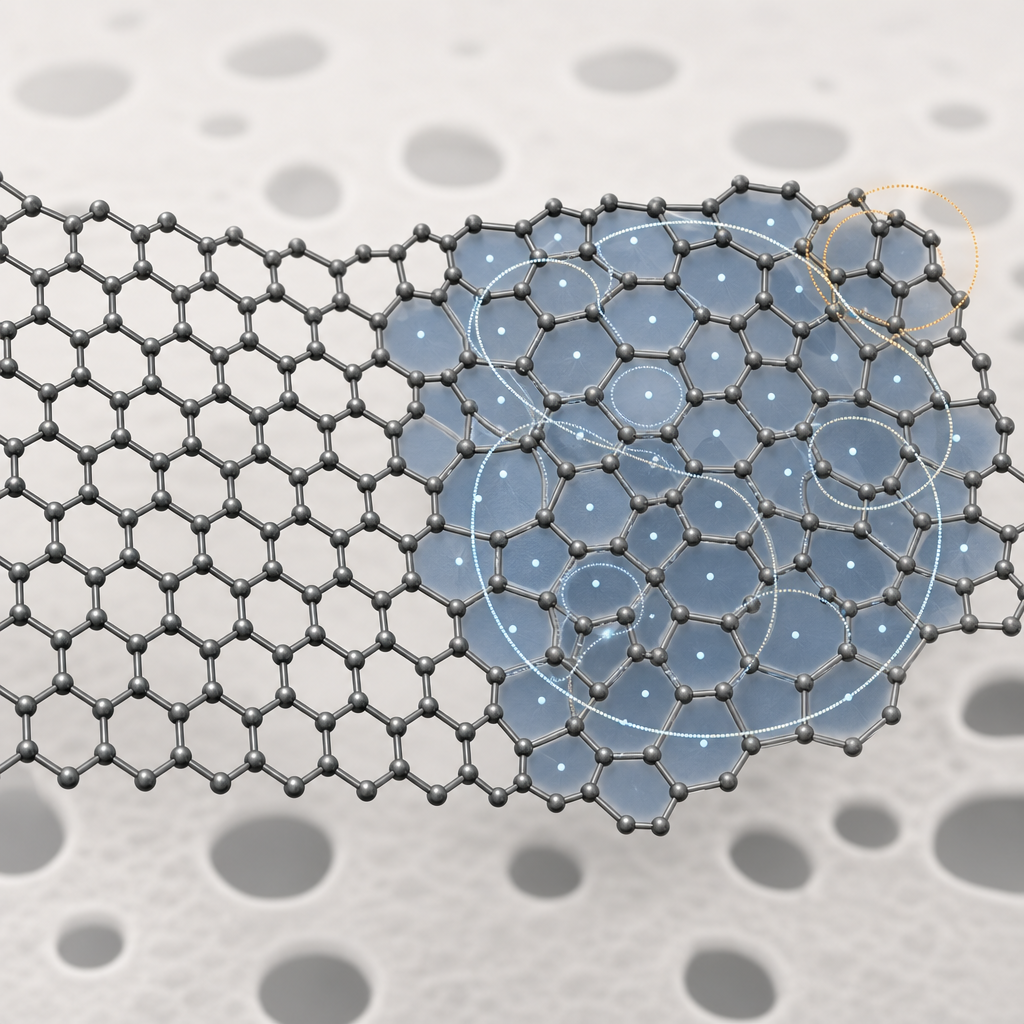
The ACS Material product appears at the very first step of the methodology. A graphene specimen was prepared by transferring commercial graphene (Trivial Transfer Graphene, ACS Materials, USA) onto a molybdenum-supported Quantifoil carbon film. The sample was heated in the microscope column to clean the surface, then observed with a JEOL JEM-ARM200F aberration-corrected microscope. To introduce lattice defects in a controlled way, the as-prepared graphene was irradiated with a 200-keV electron beam (initial dose rate 1.5 x 10^5 e- nm^-2 s^-1 for 20 s), while imaging was performed at a reduced 80-keV accelerating voltage to limit additional damage. The clean, single-layer character of the transferred graphene was essential: it provided uniform monolayer regions in which individual carbon-ring polygons could be resolved and tracked through the irradiation sequence (t0 = 0 s, t1 = 20 s, t2 = 40 s), enabling the PH analysis based on grayscale persistence diagrams (g-PDs), binarized persistence diagrams (b-PDs), and point-cloud persistence diagrams (p-PDs) computed with the HomCloud software.
The quantitative results map the progression from crystalline to disordered graphene. Zero-dimensional g-PDs extracted carbon-ring interiors as local structures; birth points coincided with polygon centers and reconstructed atomic positions via Voronoi analysis. Roundness (R) distributions ranged from 1 to over 7 with a peak near 1.6, and the fraction of holes with R > 2 rose from 34% at t0 to 48% at t1 and 63% at t2, signaling growing distortion. The non-hexagonal polygon fraction increased from 0% at t0 to 9.5% at t1 to 16.4% at t2. Average roundness for non-hexagonal polygons rose from 3.49 (hexagons at t0) to 4.49 at t1 and 4.98 at t2, while standard deviation increased with polygon number N, showing heptagons distort more readily than pentagons. One-dimensional p-PDs of downsampled hexagon-center point clouds produced large rings that reliably enclosed connected defect clusters spanning simple 5-7 and 5-8-5 defects to complex aggregates of more than twenty non-hexagonal polygons; cluster patch sizes ranged from 0.8 to 3.4 nm with up to 67 non-hexagonal polygons per patch. The average number of defects enclosed per ring grew from 4.6 to 6.5, directly quantifying interconnected defect-cluster growth under irradiation.
This topological framework enables automated, unsupervised analysis of disordered 2D materials where no characteristic length scale exists and labeled training data are scarce. It complements, and in some regimes outperforms, CNN-based segmentation (U-Net, SegNet, DeepLabv3+) for multiscale defect networks. The authors note the approach is, in principle, extensible to three dimensions when minimum structural units are simple and roughly convex, and could be combined with machine-learning loss functions for point-cloud optimization and Monte Carlo generation of amorphous atomic structures. Beyond graphene, the descriptors support defect engineering in 2D materials for electronics, thermoelectrics, and spintronics, and offer a route to predictive modeling of structure-property relationships in glassy and amorphous solids.
For researchers working on 2D-material defect characterization, the study illustrates how a clean, transferable monolayer graphene source underpins reliable atomic-scale imaging and quantitative analysis. The Trivial Transfer Graphene used here is part of ACS Material's Trivial Transfer Series, available to laboratories that need polymer-supported graphene films for easy transfer onto TEM grids, custom substrates, or device stacks. As the paper's results show, consistent monolayer quality is a prerequisite for distinguishing intrinsic structural evolution from extrinsic imaging artifacts.How ACS Material products were used
- Trivial Transfer® Graphene (Trivial Transfer Series) — “A graphene specimen was prepared by transferring commercial graphene (Trivial Transfer Graphene, ACS Materials, USA) onto a molybdenum-supported carbon film (Quantifoil, Quantifoil Micro Tools GmbH, Germany).”
Product Performance in this StudyThe Trivial Transfer Graphene served as the single-layer graphene specimen whose defects were imaged by HR-TEM and analyzed by persistent homology. It transferred cleanly onto the Quantifoil support and provided high-quality monolayer graphene whose lattice and electron-irradiation-induced defects were quantitatively characterized.
Related product categories
Frequently asked questionsWhat is Trivial Transfer Graphene used for in TEM defect studies?
In this study, Trivial Transfer Graphene served as the single-layer specimen transferred onto a Quantifoil carbon film and imaged by aberration-corrected HR-TEM. Its clean monolayer quality allowed individual carbon-ring polygons to be resolved and tracked through electron-beam irradiation, enabling persistent-homology analysis of defect formation, ring distortion, and cluster connectivity at the atomic scale.
How does persistent homology quantify graphene defects in HR-TEM images?
Persistent homology builds persistence diagrams that track topological features across scales. Zero-dimensional grayscale diagrams extract carbon-ring interiors to measure roundness and polygon number, while one-dimensional point-cloud diagrams of polygon centers produce large rings enclosing connected defect clusters. This label-free, low-hyperparameter approach quantifies both local defect geometry and global connectivity without large annotated training datasets.
How does electron-beam irradiation change graphene structure in this work?
Electron irradiation increased both the fraction of non-hexagonal polygons and their distortion. The non-hexagonal fraction rose from 0% to 9.5% to 16.4% across irradiation times, the proportion of holes with roundness above 2 grew from 34% to 63%, and the average number of defects per enclosing ring increased from 4.6 to 6.5, showing defect clusters grow in an interconnected manner.