-
Trivial Transfer Graphene for VUV Photodetectors - Argonne National Laboratory, 2023
Jul 08, 2026 | ACS MATERIAL LLCAmsterdam, S. H., Mane, A. U., & Martinson, A. B. F. (2023). Ultrathin amorphous gallium oxide vacuum ultraviolet photodetectors. *ACS Applied Electronic Materials*. https://doi.org/10.1021/acsaelm.3c00918
Argonne National Laboratory · ACS Applied Electronic Materials · 2023
Argonne National Laboratory used ACS Material Trivial Transfer Graphene as a VUV-transparent electrode on ultrathin amorphous Ga2O3 to build self-powered 120-200 nm photodetectors.
About this research
Researchers at Argonne National Laboratory used ACS Material Trivial Transfer Graphene as the VUV-transparent top electrode in self-powered Schottky-diode photodetectors built on ultrathin amorphous gallium oxide, demonstrating responsivity across the full vacuum-ultraviolet range of 120-200 nm. Reported in ACS Applied Electronic Materials (2023) by Amsterdam, Mane, and Martinson, the work extends the demonstrated spectral range of Ga2O3-based detectors well below the prior limit of 185 nm. The key device combines a 20 nm atomic-layer-deposited (ALD) amorphous Ga2O3 absorber with a 3-5 layer graphene window contact, exploiting graphene's near-transparency throughout the VUV.
Vacuum-ultraviolet detection (10-200 nm) is in growing demand for noble-liquid scintillation in rare-event physics, plasma and flame diagnostics, analytical chemistry, and space-based solar monitoring. Existing VUV detector technologies - photomultiplier tubes, microchannel plates, and AlGaN/MgF2 diodes - typically suffer tradeoffs in power, weight, area, or robustness. Gallium oxide is an attractive ultrawide-bandgap (~4.9 eV) semiconductor, but published Ga2O3 photodetectors have been almost exclusively characterized in the deep UV above 185 nm. The combination of an extremely thin, low-power absorber with a conformal VUV-transparent contact addresses both the weight constraints of space payloads and the large-area, thin-film geometry required by next-generation noble-liquid scintillation detectors.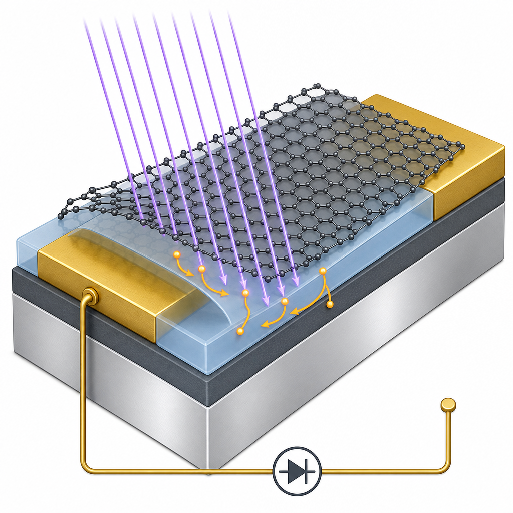
The ACS Material Trivial Transfer Graphene was deposited late in the workflow as the top electrical contact and optical window. Devices were fabricated on Si/SiO2 (300 nm thermal oxide). After thermal evaporation of 3 nm Ge / 100 nm Au pads through a Kapton shadow mask, 340 ALD cycles of trimethylgallium and ozone at 250 °C produced a 20 nm pinhole-free amorphous Ga2O3 film, with thickness verified by ellipsometry on a Si witness wafer. The 3-5 layer Trivial Transfer Graphene was then transferred onto the device per the manufacturer's instructions and cut to cover roughly half of each gold pad, forming the Schottky junction with Ga2O3 while leaving the gold exposed for ohmic contacting. Silver epoxy was used to attach lead wires to both the graphene and gold electrodes. The graphene's high transparency down to ~140 nm (with only weak features in VUV ellipsometry) is what makes top-illumination through the contact viable in this spectral window.
Amorphous Ga2O3 films grown by this ALD recipe showed strong VUV absorption across 120-200 nm, attributed to direct bandgap transitions in the amorphous network. Optical measurements were performed on MgF2 substrates under high vacuum (<5 × 10⁻⁵ Torr) using a D2 lamp, a 1200 g/mm VUV monochromator, and a sodium-salicylate-coated PMT (Hamamatsu R6095) operated at 1000 V. XPS depth profiling (Thermo K-Alpha, monochromatic Al Kα, Ar+ sputtering at ~0.13 nm/s) confirmed stoichiometric Ga2O3 throughout the film, and XRD on the as-deposited films showed the films are amorphous. The completed graphene/Ga2O3/Au Schottky diodes operated as self-powered VUV photodetectors at zero applied bias, with photocurrent measured by chopping the monochromatic VUV beam with a mechanical filter wheel. Responsivity was calculated across the full 120-200 nm window, demonstrating clear VUV photoresponse below 185 nm where Ga2O3-based detectors had not previously been characterized. The intrinsic rise time was limited to ~0.5 s by the mechanical chopper rather than by the device itself.
The combination of an ultrathin (20 nm), low-temperature, conformal ALD absorber and a flexible, VUV-transparent graphene electrode points toward lightweight, large-area VUV photodetectors compatible with space-borne solar UV instruments and with the very large active areas needed by future noble-liquid (LAr, LXe) scintillation detectors in rare-event physics. Because the Ga2O3 deposition is performed at 250 °C, the architecture is in principle compatible with a wide range of substrates, including curved or flexible surfaces. The authors note that the demonstrated spectral range of Ga2O3 photodetection now reaches well into the VUV, opening engineering optimization of contact geometry, graphene layer number, and oxide stoichiometry for improved responsivity and time response.
For groups developing wide-bandgap UV/VUV photonics, 2D-material electrodes, or thin-film optoelectronic sensors, Trivial Transfer Graphene available from ACS Material provides a polymer-supported, ready-to-transfer film of 3-5 graphene layers that, as shown here, performs as a usable VUV-transparent contact on oxide semiconductors. The product is offered alongside Trivial Transfer hexagonal boron nitride and the broader CVD graphene catalog for researchers working on photodetectors, transparent electrodes, and van der Waals device stacks.How ACS Material products were used
- Trivial Transfer® Graphene (3-5 layer) (Trivial Transfer Series) — “3-5 layer Trivial Transfer Graphene© (ACS Materials) is then transferred onto the substrates according to the manufacturer's instructions. The graphene is cut and placed on the substrates such that it covers roughly half of each gold pad.”
Product Performance in this StudyThe Trivial Transfer Graphene served as the VUV-transparent top electrode in a Schottky-diode photodetector built on ultrathin amorphous Ga2O3. Its high transparency down to ~140 nm allowed VUV photons to reach the absorber, enabling self-powered VUV detection and extending the demonstrated spectral range of gallium oxide photodetectors below 185 nm.
Related product categories
Frequently asked questionsWhy is graphene used as a top electrode in vacuum ultraviolet photodetectors?
Graphene is nearly transparent down to about 140 nm, which is essential for top-illuminated VUV detectors where photons must reach the absorber without being blocked. In this Argonne study, 3-5 layer Trivial Transfer Graphene functioned as both the Schottky contact and the optical window on amorphous Ga2O3, enabling self-powered photoresponse across the entire 120-200 nm range that conventional metal electrodes would block.
How does amorphous gallium oxide compare with crystalline beta-Ga2O3 for UV photodetection?
Amorphous Ga2O3 deposited by atomic layer deposition can be grown at relatively low temperatures (~250 °C) as conformal, pinhole-free ultrathin films, making it compatible with a wider range of substrates than beta-Ga2O3. The amorphous network still provides strong absorption throughout the deep and vacuum UV. This work shows that 20 nm amorphous Ga2O3 absorbs strongly from 120-200 nm and supports self-powered Schottky-diode photodetection.
What applications need VUV photodetectors below 185 nm?
Sub-185 nm photodetection is needed for noble-liquid (argon, xenon) scintillation detectors used in dark matter and neutrino experiments, for flame and plasma diagnostics, for VUV analytical chemistry, and for space-based solar and atmospheric monitoring. Thin, lightweight, low-power detectors are particularly valuable for space payloads and for large-area scintillation systems where weight and tiling are major constraints.