-
Trivial Transfer Graphene Photodetector - Sandia, 2017
Jul 07, 2026 | ACS MATERIAL LLCHowell, S. W. et al. (2017). Graphene-insulator-semiconductor junction for hybrid photodetection modalities. *Scientific Reports*. https://doi.org/10.1038/s41598-017-14934-4
Scientific Reports · 2017
Sandia National Laboratories built a graphene-insulator-silicon photodetector with 2,500 A/W responsivity using ACS Material Trivial Transfer Graphene.
About this research
Researchers at Sandia National Laboratories demonstrated a deeply depleted graphene-insulator-semiconductor (D2GIS) photodetector built on ACS Material Trivial Transfer Graphene that reaches visible-light responsivities as high as 2,500 A/W (25,000 S/W) and a dynamic range exceeding 30 dB. The device uses a single-layer CVD graphene channel transferred onto a HfO2-coated, low-doped silicon wafer to combine photo-charge integration in the silicon depletion region with built-in amplification provided by the graphene field-effect transistor (GFET). The result is a self-sensing analog of a depleted MOS capacitor that can be read out continuously while it is still integrating signal.
Graphene-based photodetectors face a fundamental tension: graphene absorbs broadband light, but a single atomic layer captures only a small fraction of incident photons, and photo-generated carriers recombine within roughly one micrometer. Photoconducting graphene detectors therefore typically deliver less than 100 mA/W of responsivity. Nanoantenna concentrators and bolometric architectures have improved performance but still rely on absorption within the graphene itself. The Sandia team adopts a different strategy that has gained traction in the photodetection community: use graphene only as a transparent, high-mobility charge-sensing layer and let a thicker semiconductor handle absorption. This photogating concept decouples spectral coverage from graphene's optical limitations and is directly relevant to imaging from the ultraviolet through the infrared, including non-silicon absorbers such as InAs, InSb, and HgCdTe.
The ACS Material Trivial Transfer Graphene served as the active GFET channel in this architecture. The Methods section states: "Graphene (Single Layer 1 cm × 1 cm Trivial Transfer Graphene- ACS Materials) was then transferred onto the substrate, rinsed in acetone, IPA, and then blown dry with nitrogen gas." Devices were built on 400 µm thick n-type <111> silicon with resistivity above 5,000 Ωcm. The backside was implanted with 75As+ ions, activated by rapid thermal annealing at 900 °C, and contacted with Ti/Au. On the front side, ~50 nm of HfO2 was deposited by atomic layer deposition at 250 °C as the gate dielectric. The Trivial Transfer Graphene was then placed onto this HfO2 surface, photolithographically patterned, and etched in O2 plasma. A 1.5 nm Al adhesion layer was oxidized in situ and capped with a 50 nm HfO2 passivation by ALD before Ti/Au source-drain contacts were defined. Trivial Transfer's polymer-supported, wet-release format is well suited to this kind of stack because it preserves a continuous graphene sheet across the dielectric.
The completed D2GIS devices achieved several quantitatively notable results. Under visible illumination, responsivities reached 2,500 A/W and, in optimized measurements, exceeded 2,700 A/W, with corresponding transconductance-normalized responsivities of 25,000 S/W. The dynamic range exceeded 30 dB at room temperature. The measured graphene mobility of the transferred film was 1,200 cm²/Vs, which the authors note is well below the >100,000 cm²/Vs reported in the literature for the best CVD graphene; modeling shows that pushing the mobility toward 10,000 cm²/Vs and reducing the Si/HfO2 surface generation velocity from 480 cm/s to 10 cm/s would substantially increase both responsivity and signal-to-noise ratio at short integration times. Operation was characterized with a Keithley 2400 drain bias source, a Keithley 428 fast preamp, and a National Instruments USB-6251 generating back-gate pulses with a 20 V/µs slew rate that drives the silicon into deep depletion in under 1 µs. Optical excitation used 405 nm and 635 nm Thorlabs fiber-coupled laser sources delivered through the probe-station microscope. Id(Vbg) sweeps with integration times from 640 µs to 120 ms were used to characterize transient charge integration.
Because the graphene only senses charge, the D2GIS concept transfers to arbitrary semiconductor absorbers. The authors explicitly call out indium arsenide (InAs), indium antimonide (InSb), and mercury cadmium telluride (HgCdTe/MCT) as candidate absorbers, opening pathways to mid- and long-wave infrared imaging arrays that integrate signal locally without the long-range lateral charge transport required by conventional CCDs. Applications include scientific imaging, low-light sensing, and hybrid focal plane arrays where photo-charge integration and on-pixel amplification need to coexist. The work also suggests an upgrade path: pairing higher-mobility CVD graphene with refined HfO2 ALD recipes should yield substantially better responsivity and SNR in next-generation devices.
For researchers building GFET-based photodetectors, photogated sensors, or 2D/3D hybrid imaging stacks, the relevant ACS Material product is Trivial Transfer Graphene, which provides ready-to-deposit single-layer CVD graphene on a polymer carrier that releases onto arbitrary dielectric substrates. This study illustrates a realistic baseline for the material's electrical performance on HfO2 and shows how that performance translates into a functional photodetector. The same product line, along with related CVD graphene on copper, silicon, SiO2, and quartz substrates, is available from ACS Material for groups working on photodetection, transparent electrodes, and 2D-semiconductor heterostructures.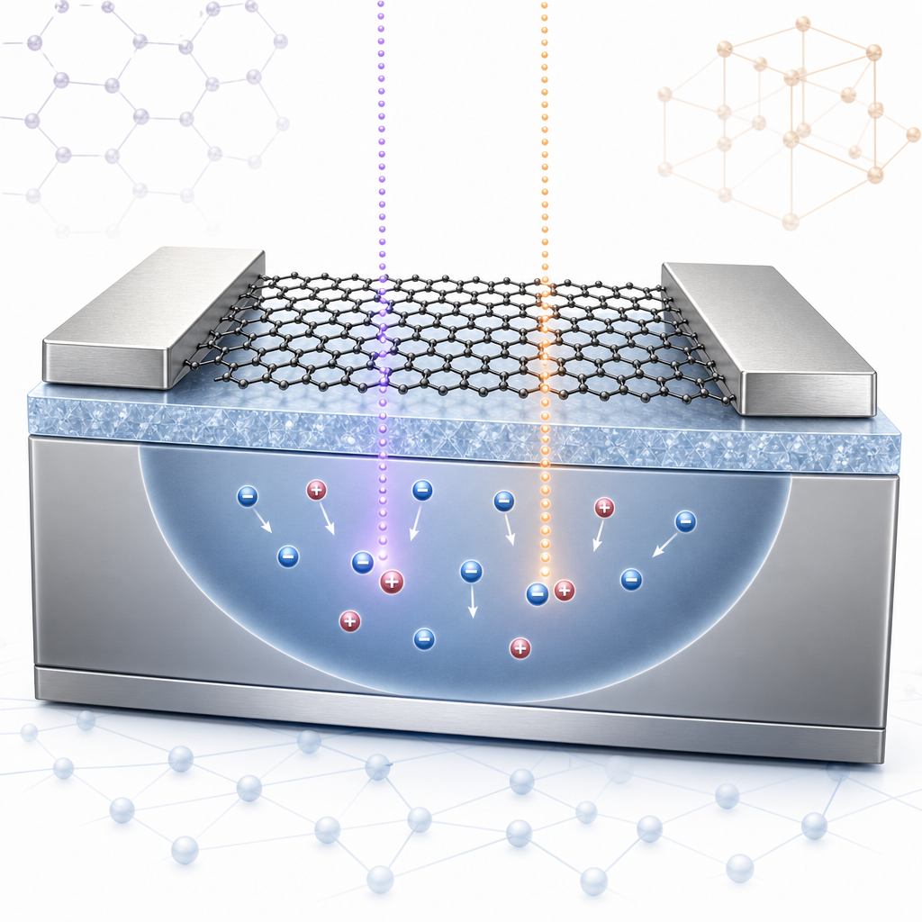
How ACS Material products were used
- Trivial Transfer® Graphene (Single Layer, 1 cm × 1 cm) (Trivial Transfer Series) — “Graphene (Single Layer 1 cm × 1 cm Trivial Transfer Graphene- ACS Materials) was then transferred onto the substrate, rinsed in acetone, IPA, and then blown dry with nitrogen gas.”
Product Performance in this Study
The Trivial Transfer Graphene formed the charge-sensing channel of the graphene field-effect transistor at the heart of the D2GIS photodetector. Devices using the transferred CVD graphene achieved responsivities up to 2,500–2,700 A/W and a 30 dB dynamic range, demonstrating that the commercially supplied film, with measured mobility of 1,200 cm²/Vs, is sufficient for functional hybrid photogating devices.
Related product categories
Frequently asked questions
How does graphene photogating improve photodetector responsivity?
In a photogating architecture, graphene is not the light absorber but a high-mobility, charge-sensing layer. Photogenerated carriers in an adjacent semiconductor capacitively couple to the graphene channel and shift its conductance. Because the source-drain current scales with graphene's high ambipolar mobility, the device gains a built-in amplification mechanism. The Sandia D2GIS device achieves up to 2,500 A/W, orders of magnitude above typical photoconducting graphene detectors below 100 mA/W.
Why use Trivial Transfer Graphene for fabricating GFET photodetectors on HfO2?
Trivial Transfer Graphene is a single-layer CVD graphene supplied on a polymer carrier that can be wet-released onto arbitrary dielectric substrates. This is critical for GFETs built on ALD-deposited HfO2, where the gate dielectric cannot survive harsh transfer chemistry. The Sandia team transferred 1 cm × 1 cm films onto 50 nm HfO2 on low-doped silicon and obtained continuous channels with 1,200 cm²/Vs mobility, sufficient to produce 2,500 A/W photoresponse.
What is the dynamic range and operational principle of a D2GIS detector?
A deeply depleted graphene-insulator-semiconductor (D2GIS) detector behaves like a self-reading depleted MOS capacitor. Photo-generated charge collects in the potential well at the Si/HfO2 interface and induces opposite-polarity charge in the graphene channel, modulating its conductance. The Sandia devices reached a 30 dB dynamic range at room temperature and integrated signal continuously while reading out, enabling new charge-integrating imaging modalities with on-pixel amplification.