-
Trivial Transfer Graphene Photodetectors — Sandia National Laboratories, 2019
Jun 25, 2026 | ACS MATERIAL LLCRuiz, I. et al. (2019). Interface defect engineering for improved graphene-oxide-semiconductor junction photodetectors. *ACS Applied Nano Materials*. https://doi.org/10.1021/acsanm.9b00978
Sandia National Laboratories · ACS Applied Nano Materials · 2019
Sandia National Laboratories used ACS Material Trivial Transfer® graphene to build D2GOS photodetectors and study how interface defects govern photoresponsivity.
About this research
Researchers at Sandia National Laboratories used ACS Material Trivial Transfer® CVD single-layer graphene to fabricate dielectric-double-gated graphene-oxide-semiconductor (D2GOS) junction photodetectors, demonstrating that the interface defect density at the silicon/dielectric boundary directly determines photoresponse behavior. The team built four device variants spanning interface defect densities (Dit) from roughly 1.7×10¹³ down to 2×10¹¹ eV⁻¹cm⁻², using reactive ion etch, buffered oxide etch, and thermal-oxide passivation strategies. Their results, published in ACS Applied Nano Materials in 2019, link Dit and substrate polarity to graphene doping type, band bending, and ultimately to detector gain and responsivity.
Graphene-on-semiconductor photodetectors are attractive because graphene's high carrier mobility enables internal gain, while the underlying silicon absorber provides broadband sensitivity and CMOS compatibility. However, the performance of these hybrid junctions is notoriously sensitive to the buried oxide/silicon interface, where trapped charge can pin the Fermi level, shift threshold voltages, and degrade responsivity. The community has lacked a systematic study correlating quantified Dit values with photodetector output for graphene-gated junctions. This work fills that gap by holding the graphene source and dielectric stack thickness essentially constant while tuning the interface treatment, isolating the role of defect engineering on device behavior in the dielectric-double-gated configuration.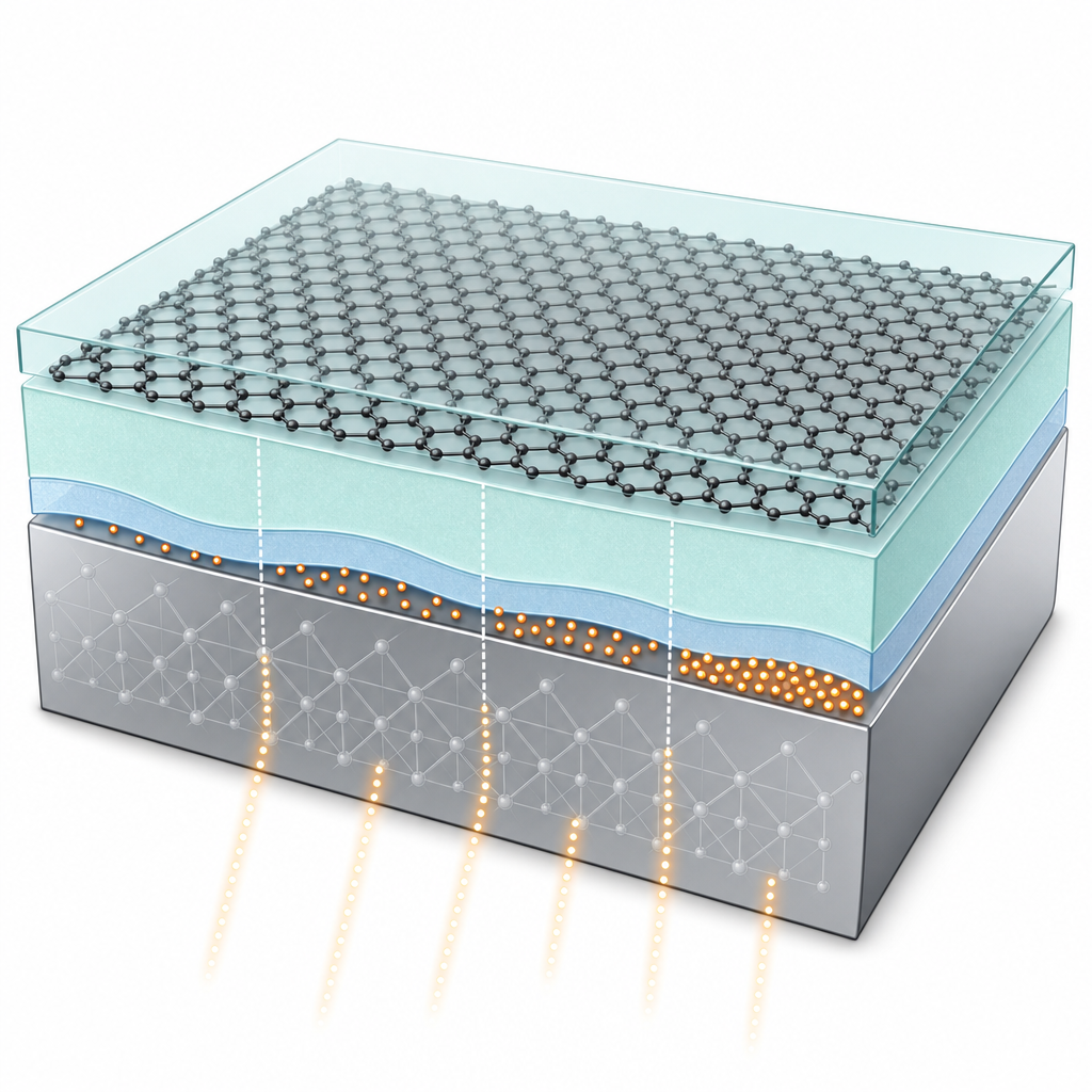
The ACS Material Trivial Transfer® graphene was the top gate/electrode of every device. After silicon surface treatment and 50 nm HfO2 atomic layer deposition (plus an optional 15 nm thermal SiO2 buffer), the CVD single-layer graphene was wet-transferred onto the dielectric stack, patterned into 200 µm × 250 µm pixel arrays, contacted with metal electrodes, and passivated by an additional HfO2 ALD overlayer. The authors explicitly note in their Experimental section: "chemical vapor deposited single layer graphene films (ACS Materials, Trivial Transfer) were wet transferred, patterned … and then passivated." Because Trivial Transfer® supports clean wet-transfer onto arbitrary dielectric surfaces without requiring users to grow their own graphene, it was well matched to a process flow that demanded identical graphene quality across four interface variants.
Key results. Capacitance–voltage measurements on companion MOS structures established the four Dit regimes: high (HID, 1–1.7×10¹³ eV⁻¹cm⁻², RIE-treated n-type (111) Si, >5,000 Ω·cm), moderate (MID, 0.75–5×10¹² eV⁻¹cm⁻², BOE-treated (111) Si), low p-type (pLID, 0.4–1×10¹² eV⁻¹cm⁻², n-type (100) Si with 15 nm thermal SiO2), and low n-type (nLID, 2–5×10¹¹ eV⁻¹cm⁻², p-type (100) Si with 15 nm thermal SiO2). Graphene Hall mobilities on the finished devices ranged from 523 cm²/V·s on the HID stack to 909 cm²/V·s on the MID stack, with 637 and 884 cm²/V·s for the pLID and nLID respectively. The dielectric constants of the stacks were near 15 for the HfO2-only devices and ~11.3 for the SiO2/HfO2 stacks. Importantly, the sign of the accumulated charge in the silicon flipped graphene's effective doping: HID and MID stacks produced n-type graphene, while the lower-defect SiO2-buffered stacks produced p-type graphene. The authors show that this Dit-driven Fermi-level positioning, rather than bulk dark-carrier generation (diffusion lengths remained on the order of millimeters across the resistivity range), governs the device's photoresponse and gain.
Applications and outlook. Engineering the buried interface to tune graphene's working point opens a deterministic route to optimize D2GOS detectors for visible and near-infrared imaging, low-light photodetection, and integrated photonic receivers. The same principles transfer to other graphene-gated devices including phototransistors for short-wave infrared, hybrid graphene–silicon CMOS image sensors, and chemical/biosensing field-effect platforms where the buried dielectric quality dictates sensitivity. The paper points toward follow-up work that combines defect engineering with bandgap-tuned absorbers and with bias-controlled gain to push detectivity, while keeping fabrication compatible with standard silicon foundry steps.
For researchers reproducing this kind of graphene-on-dielectric device, the relevant material is available from ACS Material as Trivial Transfer® graphene, a CVD single-layer graphene supplied on a transfer support designed for wet transfer onto user-defined substrates. The Sandia results are a useful benchmark: device-grade D2GOS junctions with graphene mobilities in the 500–900 cm²/V·s range are achievable from this product when paired with appropriately prepared HfO2 and SiO2/HfO2 dielectric stacks.How ACS Material products were used
- Trivial Transfer® Graphene (Trivial Transfer Series) — “chemical vapor deposited single layer graphene films (ACS Materials, Trivial Transfer) were wet transferred, patterned (200 µm x 250 µm pixel arrays) and then passivated via an additional HfO2 ALD deposition”
Product Performance in this StudyThe Trivial Transfer® CVD graphene served as the top electrode of the D2GOS photodetector junctions. Wet-transferred films delivered measured sheet mobilities between 523 and 909 cm²/V·s, sufficient to support the gain mechanism in the photodetectors across all four interface-engineered device variants.
Related product categories
Frequently asked questionsWhat is Trivial Transfer graphene used for in photodetector research?
Trivial Transfer graphene is a CVD single-layer graphene film designed for wet transfer onto arbitrary substrates, making it well suited to building graphene-on-dielectric photodetectors. In the Sandia D2GOS study it served as the optically transparent top electrode on HfO2 and SiO2/HfO2 stacks, contributing carrier mobilities of 523–909 cm²/V·s and enabling the internal gain mechanism that gives these detectors their photoresponse.
How does interface defect density affect graphene-on-silicon photodetector performance?
Interface defects at the silicon/dielectric boundary trap charge and shift the graphene Fermi level, which directly changes the band bending in the underlying silicon. The Sandia work shows that going from Dit ~1.7×10¹³ to ~2×10¹¹ eV⁻¹cm⁻² flips the effective graphene doping between n-type and p-type and reshapes the photoresponse, making interface engineering a primary lever for D2GOS detector optimization.
Why use HfO2 with a thin thermal SiO2 buffer in graphene photodetectors?
HfO2 deposited by ALD provides a high-k dielectric that enables strong field coupling between graphene and the silicon absorber, but ALD-HfO2 directly on silicon often produces a high density of interface traps. Adding a 15 nm thermally grown SiO2 buffer dramatically lowers Dit to the 10¹¹–10¹² eV⁻¹cm⁻² range, preserving high gate coupling while reducing Fermi-level pinning and dark-current variability.