-
Ag Nanowire-Doped Graphene Self-Powered Photodetectors - Kyung Hee University, 2018
Jun 23, 2026 | ACS MATERIAL LLCShin, D. H. et al. (2018). Self-powered Ag-nanowires-doped graphene/Si quantum dots/Si heterojunction photodetectors. *Journal of Alloys and Compounds*.
Journal of Alloys and Compounds · 2018
Kyung Hee University researchers used ACS Material silver nanowires to dope CVD graphene in Si quantum dot heterojunction photodetectors with 85% EQE at zero bias.
About this research
Researchers at Kyung Hee University used silver nanowires (Ag NWs) purchased from ACS Material to dope CVD-grown graphene transparent conductive electrodes in self-powered Ag-NW-doped graphene/p-type Si quantum dot (SQD):SiO2/n-Si heterojunction photodetectors, achieving a photocurrent/dark current on/off ratio of 10^5 at zero applied bias, 94.2% external quantum efficiency, and 4.5 × 10^12 cm·Hz^1/2/W specific detectivity in the visible range. Published in the Journal of Alloys and Compounds (2018), the work demonstrates that combining a doped graphene electrode with a silicon quantum dot absorption layer can deliver photodetector performance competitive with commercial silicon photodiodes without requiring an external bias.
Broadband photodetectors that span the UV to IR range are central to imaging, communications, environmental sensing, and biomedical instrumentation. Graphene/Si heterojunctions are appealing because they offer strong photoresponse across the visible spectrum, but bare graphene/Si interfaces typically suffer from Fermi-level pinning and large leakage currents that limit detectivity and response speed. Most graphene/Si photodetectors also require an external bias to operate, which complicates integration into low-power and remote sensing systems. Embedding p-type silicon quantum dots in a SiO2 matrix between the graphene electrode and n-Si substrate addresses both problems: it enhances visible-light absorption through quantum confinement and provides a built-in photovoltaic field that supports zero-bias (self-powered) operation. The remaining challenge is to make the graphene electrode conductive and band-aligned enough to efficiently extract photogenerated carriers, which motivates n-type doping of the graphene with metallic nanowires.
In the device workflow, monolayer graphene grown by chemical vapor deposition on copper foil was transferred onto a 120 nm p-SQD:SiO2/n-Si heterojunction substrate. The Ag nanowires from ACS Material had 99.5% purity and a 70 nm average diameter. They were dispersed in isopropyl alcohol at concentrations ranging from 0.05 to 0.3 wt%, drop-cast onto the graphene-covered substrate, spin-coated at 1500 rpm for 1 minute, and dried at 100 °C for 2 minutes. Aluminum and InGa films served as the top and bottom electrodes, respectively. Field-emission SEM showed that increasing Ag NW concentration produced denser nanowire networks on the graphene surface, while XPS of the C 1s, Ag 3d, and O 1s peaks confirmed successful surface doping without C–Ag covalent bonding, indicating that the Ag NWs dope graphene through physical contact and charge transfer rather than chemical modification.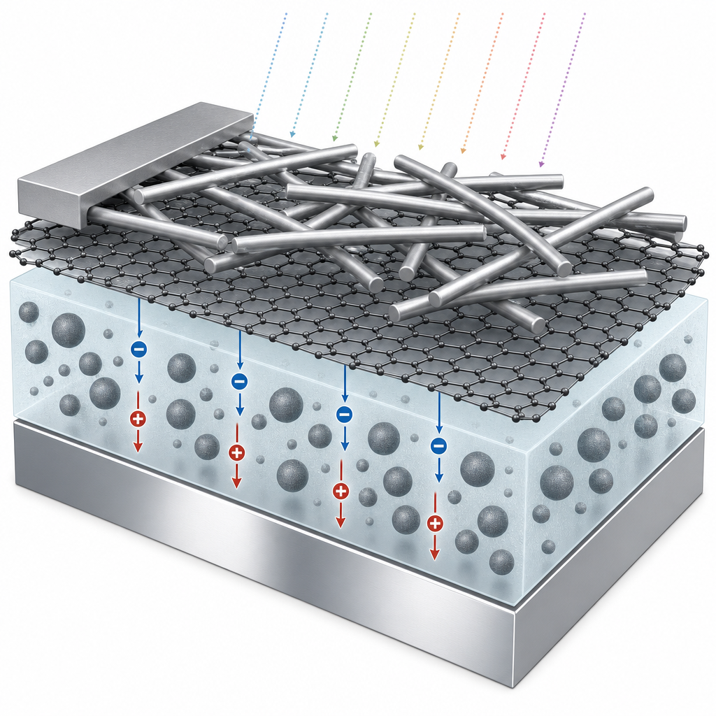
The Ag NW doping monotonically shifted the graphene work function from 4.52 ± 0.047 eV (pristine) to 4.33 ± 0.022 eV at 0.3 wt%, confirming n-type behavior. Sheet resistance dropped sharply from ~845 Ω/sq for undoped graphene to 92 Ω/sq at 0.1 wt% and 55 Ω/sq at 0.3 wt%, while transmittance at 550 nm decreased by only about 12% at the highest loading. The figure of merit σDC/σOP peaked at 45.6 for 0.1 wt% Ag NWs, exceeding the industry benchmark of 35. Carrier mobility decreased from 2895 ± 160 to 1706 ± 98 cm^2/V·s with doping, reflecting added scattering. For the optimized 0.1 wt% device, dark current was suppressed and the shunt resistance reached 14,906 Ω·cm^2. Photodetector metrics included responsivity of 0.32–0.65 A/W across 500–900 nm, ~85% EQE (up to 94.2% peak), 4.5 × 10^12 cm·Hz^1/2/W detectivity, an 83 dB linear dynamic range at 532 nm, and a response time of ~2 ms. The detectors retained 85% of their initial responsivity after 700 hours in ambient air, indicating robust operational stability.
The demonstrated zero-bias performance positions these devices for low-power optoelectronic applications, including wearable and remote sensors, imaging arrays, optical communication receivers, and integrated visible-light detection where battery-free operation is desirable. Because the EQE in the visible range is comparable to commercial silicon photodiodes and exceeds previously reported graphene/Si photodetectors, the architecture is also relevant to next-generation photovoltaic-photodetector hybrid devices. The authors highlight that the same Ag NW-doped graphene/SQD/Si platform could be extended to broadband self-powered detectors and to flexible substrates, given the mechanical compliance of nanowire networks and CVD graphene films.
For researchers developing graphene-based transparent electrodes, transparent conductors for solar cells, or silicon-compatible photodetectors, the silver nanowires used here are available from ACS Material as part of the nanowire product line. The study provides a useful reference point for the doping concentration window, sheet resistance versus transmittance trade-off, and device stability that can be expected when integrating Ag NWs with monolayer graphene on silicon-based heterojunctions.How ACS Material products were used
- Silver Nanowires (70 nm average diameter, 99.5% purity) (Nanowire Series) — “Ag NWs (purity: 99.5%) of 70 nm average diameter were purchased from ACS material.”
Product Performance in this StudyAg nanowires acted as an n-type dopant for the CVD graphene transparent conductive electrode, lowering sheet resistance from ~845 to 92 Ω/sq at 0.1 wt% loading and enabling self-powered photodetector operation with on/off ratio of 10^5, ~85% EQE, and 4.5 × 10^12 cm·Hz^1/2/W detectivity.
Related product categories
Frequently asked questionsHow do silver nanowires improve graphene transparent conductive electrodes?
Silver nanowires act as n-type dopants for CVD graphene by donating electrons through physical contact, lowering the work function and creating a percolating conductive network on the graphene surface. In this study, 0.1 wt% Ag NW doping reduced graphene sheet resistance from ~845 to 92 Ω/sq while keeping transmittance above 91% at 550 nm, yielding a σDC/σOP figure of merit of 45.6 that exceeds the 35 industry benchmark.
What enables self-powered operation in graphene/Si quantum dot photodetectors?
Embedding p-type silicon quantum dots in a SiO2 matrix between the n-type-doped graphene and n-Si substrate forms a p-n heterojunction with a strong built-in electric field. This field separates photogenerated electron-hole pairs without any applied bias, producing a photocurrent at 0 V. The reported device achieved a 10^5 on/off ratio, ~85% external quantum efficiency, and 4.5 × 10^12 cm·Hz^1/2/W detectivity under zero bias.
Why is the σDC/σOP ratio important for transparent conductive electrodes?
The σDC/σOP ratio captures the trade-off between sheet resistance and optical transmittance that any transparent conductor must balance. Higher values mean a film conducts well while still letting light through. For touchscreens, solar cells, and photodetector electrodes, an industry-accepted minimum is about 35. The Ag NW-doped graphene optimized in this work reached 45.6 at 0.1 wt% loading, making it competitive with commercial transparent conductors.