-
Cu Nanowires for Si Anode Li-Ion Batteries - UNIST, 2015
Jul 07, 2026 | ACS MATERIAL LLCHwang, C. et al. (2015). All-in-One assembly based on 3D-Intertangled and cross-Jointed architectures of Si/Cu 1D-Nanowires for lithium ion batteries. *Scientific Reports*. https://doi.org/10.1038/srep08623
Scientific Reports · 2015
UNIST researchers used ACS Material copper nanowires to build a binder-free 3D Si/Cu nanowire all-in-one separator-electrode-current collector for Li-ion batteries.
About this research
Researchers at Ulsan National Institute of Science and Technology (UNIST) used copper nanowires supplied by ACS Material to construct an all-in-one separator-electrode-current collector assembly (SECA) for lithium-ion batteries, demonstrating that intertangled Si/Cu 1D-nanowire architectures can replace conventional binders, conductive additives, and metal foil current collectors in a single integrated structure. Published in Scientific Reports in 2015 by Hwang and co-workers in the School of Energy and Chemical Engineering, the work shows that mechanical entanglement combined with ductile Cu-nanowire joints can hold a silicon-based anode together while accommodating the massive volume changes that normally pulverize Si electrodes. The result is a binder-free architecture that simultaneously addresses energy density, mechanical integrity, and electrical connectivity.
Silicon is one of the most attractive next-generation anode materials for lithium-ion batteries because its theoretical capacity (~4,000 mAh g⁻¹) is roughly ten times that of graphite (372 mAh g⁻¹). However, lithiation drives ~400% volumetric expansion, leading to particle pulverization, loss of electrical contact, unstable SEI growth, and rapid capacity fade. Conventional remedies—porous or hollow Si particles, carbon coatings, conducting polymers, or specialized polymeric binders—add inactive mass and complicate fabrication. There is therefore strong interest in binder-free, current-collector-free electrode architectures for electric vehicles and stationary storage. This work tackles that challenge by using two complementary 1D nanostructures whose mechanical entanglement provides both conductive pathways and void space for Si expansion, eliminating the need for polymer binders and heavy Cu foil.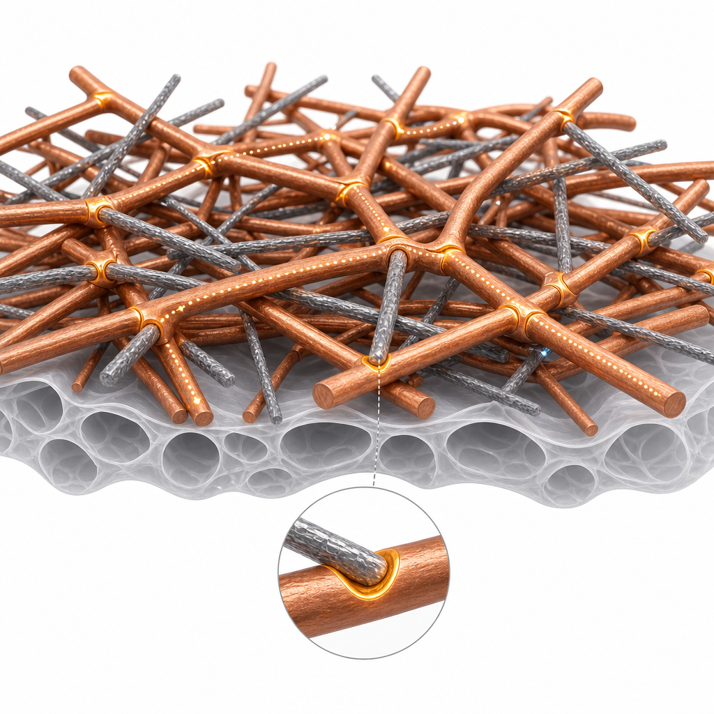
The ACS Material copper nanowires were the structural backbone of the assembly. As reported in the Methods section, the team used "nwCu (D = 100–200 nm, L = 0.8 to 6 μm, ACS material)" together with silicon nanowires (D ≈ 40 nm, L = 1–20 μm). The two nanowire populations were co-dispersed in 20 mL ethanol by ultrasonication for 30 min, then vacuum-filtered directly onto a polyethylene separator (Asahi NH716). A second filtration of an ethanolic Cu-nanowire dispersion deposited an additional Cu-nanowire layer on top of the active layer to act as an ultra-light porous current collector. After drying at 70 °C and uniaxial pressing at 12 MPa, the ductile Cu nanowires deformed into concave seats around the Si nanowires, locking the network together at "cross-joint" contact points. Tuning the nwSi:nwCu ratio controls the density of conductive contacts and the void volume available for Si expansion.
The resulting SECA showed clear quantitative advantages over a conventional Cu-foil electrode using a PAA/CMC binder and Super P carbon black at a 65:25:2 ratio with ~0.6 mg cm⁻² loading. The intertangled Si/Cu network demonstrated superior cyclability and rate capability, with the authors reporting effectively "zero volume expansion" at the electrode level because internal voids absorb the Si lithiation strain without macroscopic swelling. The all-in-one configuration removes the 18 μm Cu foil current collector and replaces the polymer binder with mechanically interlocked metallic contacts, raising the active-material fraction of the cell and therefore the gravimetric energy density. The Cu nanowires also provide continuous electronic pathways, so even Si fragments produced by cycling remain wired into the network. The combination of high-aspect-ratio entanglement, ductile metal joints, and engineered void fraction is presented as a generalizable design rule for 1D/1D composite electrodes.
The architecture has direct implications for high-energy lithium-ion batteries targeted at electric vehicles, drones, and grid storage, where both gravimetric and volumetric capacity matter. Beyond Si anodes, the cross-jointed nanowire concept could be extended to other high-capacity alloying anodes such as Sn or Ge, to conversion-type oxides, and even to flexible or wearable battery formats where the integrated separator/electrode/current-collector laminate eliminates rigid metal foils. The authors specifically highlight tunability: by adjusting the nwSi:nwCu ratio, designers can trade off conductivity, mechanical robustness, and void volume for a given application.
For researchers and engineers working on silicon anodes, binder-free electrodes, or freestanding battery components, ACS Material's copper nanowires are available in the Nanowire Series with controlled diameters and lengths comparable to those used in this study. The paper provides an example of how a commercial 1D Cu nanowire product can serve simultaneously as binder, conductive additive, and current collector when integrated with active materials in a vacuum-filtered, mechanically pressed laminate.How ACS Material products were used
- Copper Nanowire (50-200nm) (Nanowire Series) — “nwCu (D = 100 ~ 200 nm, L = 0.8 to 6 um, ACS material; Figure S7)”
Product Performance in this StudyThe copper nanowires from ACS Material served simultaneously as conductive pathway, binder substitute (via ductile structural joints), and porous current collector in the binder-free SECA architecture, enabling stable cycling of Si anodes.
Related product categories
Frequently asked questionsHow do copper nanowires replace binders and current collectors in silicon lithium-ion battery anodes?
Copper nanowires are ductile, so under uniaxial pressure they deform around silicon nanowires and form interlocking cross-joints that hold the electrode together without polymer binder. A second filtered layer of Cu nanowires on top of the active film acts as an ultra-light porous current collector, replacing the heavy Cu foil. The result is a binder-free, foil-free 3D conductive network that maintains contact even after Si volume expansion.
Why is a 3D intertangled Si/Cu nanowire network better than a conventional silicon slurry electrode?
A conventional Si slurry electrode relies on polymer binders and Super P carbon coated onto Cu foil, all of which add inactive mass and fail when silicon expands ~400 percent during lithiation. The intertangled Si/Cu nanowire architecture provides internal void space to accommodate that expansion, continuous metallic conduction paths through the Cu nanowires, and mechanical integrity through entanglement, yielding superior cyclability and rate performance with higher active-material loading.
What dimensions of copper nanowires were used in this Si/Cu battery study?
The authors used copper nanowires from ACS Material with diameters of 100 to 200 nm and lengths of 0.8 to 6 micrometers, dispersed together with silicon nanowires (about 40 nm diameter, 1 to 20 micrometers long) in ethanol. The dispersion was vacuum-filtered onto a polyethylene separator and then pressed at 12 MPa to lock the nanowire network through ductile Cu cross-joints.