-
CVD Graphene EGFET Sensor Arrays - MIT, 2016
Jun 30, 2026 | ACS MATERIAL LLCMackin, C., & Palacios, T. (2016). Large-scale sensor systems based on graphene electrolyte-gated field-effect transistors. *Analyst*.
Analyst · 2016
MIT researchers built a 256-device graphene electrolyte-gated FET sensor array with 100% yield using PMMA-coated CVD graphene from ACS Material.
About this research
Researchers at the Massachusetts Institute of Technology used PMMA-coated CVD graphene supplied by ACS Material to build a 16 × 16 array of 256 graphene electrolyte-gated field-effect transistors (EGFETs) that achieved 100% device yield and enabled, for the first time, large-sample statistical analysis of graphene EGFET electrical performance. Reported in Analyst (2016) by Charles Mackin and Tomás Palacios, the work pairs this large-scale sensor chip with a compact, self-contained measurement system that DC-characterizes all 256 devices as a function of V_DS and V_GS in a matter of minutes, and introduces a piecewise compact DC model that fits 87% of the measured I_DS–V_GS curves with a mean error of 7% or less.
Graphene EGFETs are attractive for chemical and biological sensing because graphene combines high carrier mobility, chemical inertness, a wide electrochemical potential window in physiological buffers, transparency, and mechanical flexibility, while chemical vapor deposition makes large-area films economically viable. However, prior studies were typically limited to a few tens of devices per chip, leaving the statistics of device-to-device variability — and the underlying spread in mobility, contact resistance, minimum carrier concentration n_o, and Dirac point V_o — essentially uncharacterized. Without those distributions, designing reliable large-area sensor arrays for electrogenic cell recording or chemical detection has been guesswork. This paper closes that gap by combining a wire-efficient N² × 2N array architecture, automated multiplexed readout, and a tractable compact model.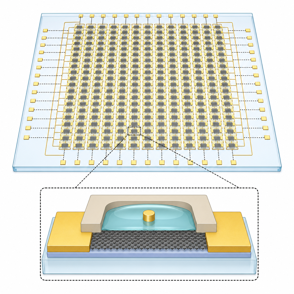
The ACS Material CVD graphene plays the central material role: it is the transistor channel. After patterning two Ti/Au (10/150 nm) interconnect layers separated by 25 nm ALD-deposited Al₂O₃ on a 0.2 mm coverslip, the authors transferred the commercial graphene/PMMA film from ACS Material across the entire array. The film was nitrogen-dried, baked 15 min at 80 °C and 2 h at 130 °C to reflow the PMMA and promote adhesion, then PMMA-stripped in acetone and annealed for 3 h at 350 °C in 700 sccm H₂ / 400 sccm Ar to remove residue. Channels were defined using an MMA/SPR3012 stack and oxygen plasma etching, and an ~2.4 μm SU-8 passivation layer with windows over each channel was patterned to localize electrolyte gating. The uniformity and cleanliness of the ACS Material graphene transfer was a prerequisite for the 100% device yield reported across all 256 transistors.
Devices were characterized in 100 mM aqueous NaCl using a Au pseudoreference gate, with V_DS swept from 10 to 150 mV and V_GS from −0.5 to 0.7 V. The compact piecewise model — derived by neglecting saturation velocity, approximating quantum capacitance with a constant top-gate capacitance C_TOP ≈ 3 μF cm⁻², and assuming symmetric contact resistance — fit 87% of devices with ≤7% mean percent error at V_DS = 150 mV. Extracted parameter distributions gave mean mobility μ = 463 ± 208 cm² V⁻¹ s⁻¹, contact resistance R_C = 6.3 ± 3.3 kΩ μm, minimum carrier concentration n_o = (1.2 ± 0.4) × 10¹² cm⁻², and Dirac point V_o = −35 ± 19 mV — values consistent with previous single-device reports. Correlation analysis revealed an inverse correlation between mobility and n_o (−0.52), and positive correlations between R_C and both μ (0.53) and n_o (−0.55 with respect to R_C inversely). The authors then translate the model into an application-specific optimization framework for intrinsic voltage gain G_V, showing how channel length, V_DS, C_TOP, R_C, and n_o can be co-optimized for electrogenic cell amplifiers.
The demonstrated architecture is directly relevant to multiplexed biosensing platforms: neural and cardiac electrogenic cell recording, ion sensing, DNA hybridization detection, immunoassays on flexible substrates, and large-area chemical sensor skins. Because the same N² × 2N wiring strategy and compact model can be ported to other 2D-material EGFETs, follow-up work could extend the platform to MoS₂, WS₂, or h-BN heterostructure channels for selectivity engineering. The framework also provides a quantitative route for fabs to monitor how process changes — anneal conditions, dielectric thickness, contact metallurgy — shift entire parameter distributions, not just single-device figures of merit.
For researchers building graphene biosensor arrays, transparent electrodes, or flexible electronics, this paper is a strong reference point that the wafer-scale CVD graphene products in ACS Material's catalog, including PMMA-coated graphene on copper foil, can support 100%-yield device fabrication when paired with a clean transfer and anneal workflow. The compact model and statistical methodology in the paper provide a reusable toolkit for translating that material quality into predictable, optimized sensor arrays.How ACS Material products were used
- CVD Graphene on Copper-PMMA Coated (CVD Graphene) — “Commercial graphene covered in poly methyl methacrylate (PMMA) from ACS Material is transferred over the array and nitrogen dried to remove any underlying water.”
Product Performance in this StudyThe PMMA-coated CVD graphene from ACS Material served as the semiconducting channel for all 256 electrolyte-gated field-effect transistors in the array, enabling 100% device yield and uniform electrical performance across the entire chip.
Related product categories
Frequently asked questionsWhy use PMMA-coated CVD graphene for electrolyte-gated transistor arrays?
PMMA-coated CVD graphene allows large-area, contamination-free transfer of a continuous monolayer onto pre-patterned electrodes. In this MIT study, the PMMA support film from ACS Material kept the graphene mechanically intact during transfer across a 16 × 16 electrode array; after baking to reflow the PMMA and an H₂/Ar anneal at 350 °C, the residual polymer was removed, leaving a uniform channel that yielded 100% working devices out of 256 fabricated.
What are typical mobility and contact resistance values for CVD graphene EGFETs?
Across 256 transistors measured in 100 mM NaCl with an Au pseudoreference gate, the MIT team extracted a mean hole/electron mobility of 463 ± 208 cm² V⁻¹ s⁻¹ and a contact resistance of 6.3 ± 3.3 kΩ μm. Mean minimum carrier concentration was 1.2 × 10¹² cm⁻² and the Dirac point sat at −35 ± 19 mV, consistent with literature values for CVD-grown graphene transferred onto Al₂O₃-coated substrates.
How does contact resistance affect graphene EGFET voltage gain?
Lower contact resistance increases transconductance while having little impact on output conductance, so the intrinsic voltage gain rises. The effect is strongest at short channel lengths, where contact resistance dominates the source–drain resistance budget. The authors recommend minimizing R_C whenever possible, since it is a parasitic that provides no benefit, and show that gain can also be raised by increasing V_DS, C_TOP, or channel length, or by decreasing minimum carrier concentration n_o.