-
CVD Graphene on Quartz for Laser Thinning - Univ. Nebraska, 2015
Jun 25, 2026 | ACS MATERIAL LLCLi, D. W. et al. (2015). In situ imaging and control of layer-by-layer femtosecond laser thinning of graphene. *Nanoscale*. https://doi.org/10.1039/c4nr07078j
Department of Electrical and Computer Engineering · Nanoscale · 2015
University of Nebraska-Lincoln researchers used ACS Material CVD graphene on quartz to demonstrate femtosecond laser layer-by-layer graphene thinning with atomic precision.
About this research
Researchers at the University of Nebraska-Lincoln demonstrated layer-by-layer femtosecond (fs) laser thinning of graphene using, among their samples, commercial few-layer CVD graphene on a quartz substrate purchased from ACS Material, achieving single-atomic-layer thinning precision monitored in real time by four-wave mixing (FWM) imaging. The team showed that an 800 nm Ti:Sapphire fs laser configured within an FWM optical system can both thin graphene and image it simultaneously, exploiting graphene's large optical nonlinearity. A linear relationship between FWM signal intensity and graphene layer number provided a fast, quantitative way to count layers and track removal as it happened. The work addresses the long-standing challenge of producing graphene with a controlled, on-demand number of layers.
Graphene's electronic, thermal, and mechanical properties depend strongly on the number of layers: thermal conductivity, work function, hydrogenation behavior, and the metal-to-semiconductor transition all vary with thickness. Despite mature growth routes such as CVD, mechanical exfoliation, and solution-phase synthesis, precise thickness control remains difficult. Prior laser-thinning approaches using continuous-wave (CW) lasers relied on oxidative burning and could typically reach only trilayer or monolayer endpoints, with limited intermediate control. Alternative methods such as zinc sputter-coating followed by acid dissolution are slow and risk contamination. A technique capable of removing graphene one atomic layer at a time, while simultaneously verifying thickness, would benefit transistors, transparent conducting electrodes, optoelectronics, Hall-effect sensors, and other devices where layer count dictates performance.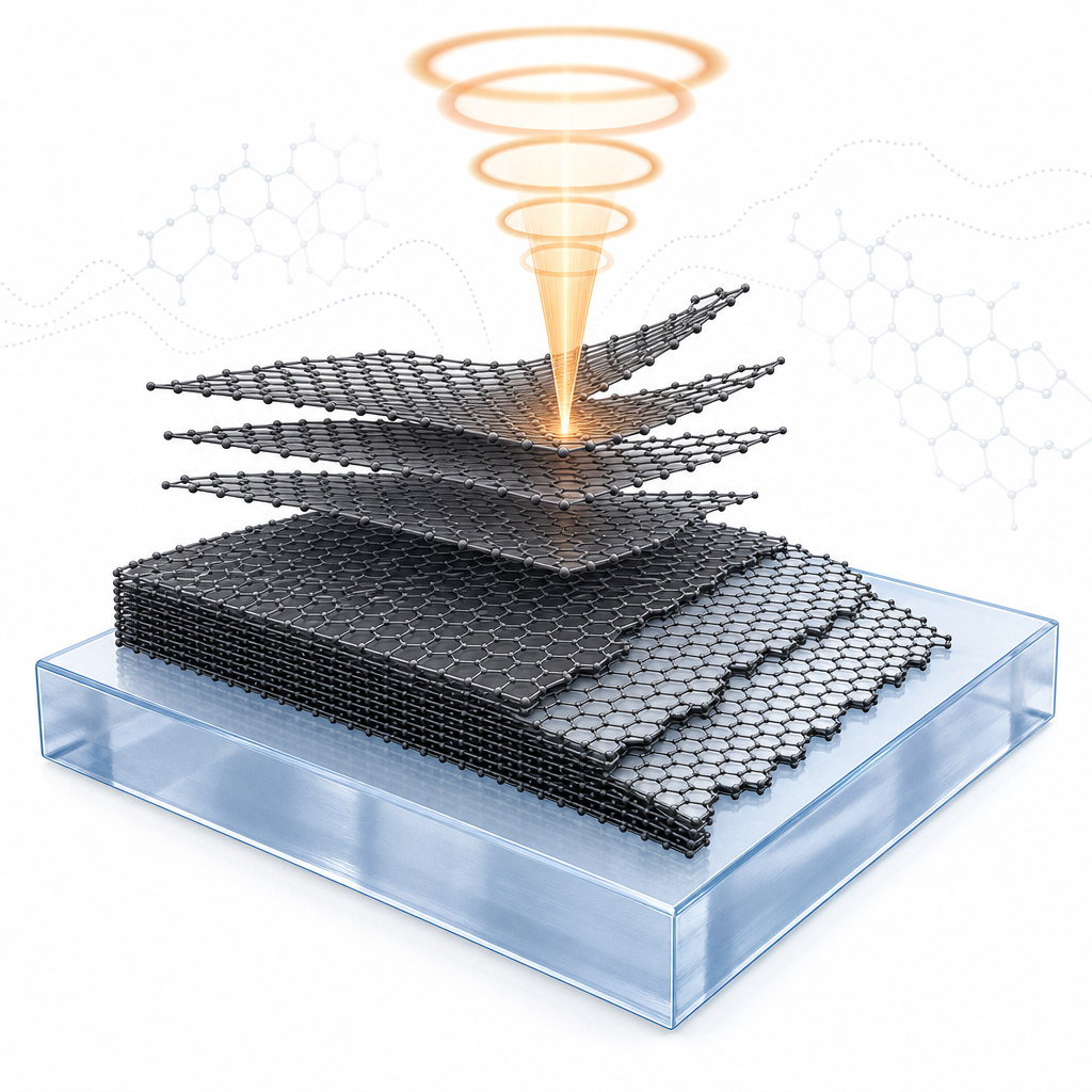
Three graphene sample types were studied: commercial few-layer CVD graphene on a quartz substrate (six to eight layers) purchased from ACS Material; rapid-thermal-processing (RTP) graphene grown on fused silica from amorphous carbon and nickel films; and micromechanically cleaved few-layer graphene from highly oriented pyrolytic graphite (HOPG). The ACS Material CVD graphene was transferred onto a quartz substrate and characterized by FWM imaging alongside the other samples (Figs. 2b-d). Although the physical appearance of CVD, RTP, and exfoliated graphene differed, all produced clear FWM signals, confirming similar nonlinear optical responses and validating FWM as a universal imaging contrast mechanism for few-layer graphene. The CVD-on-quartz sample thus established that commercially sourced material behaves equivalently to lab-grown films in the nonlinear-optical measurement, an important control for generalizing the layer-counting calibration. Characterization combined atomic force microscopy (AFM), Raman spectroscopy (514 nm excitation, Renishaw InVia), and the FWM system built around a MaiTai DeepSee Ti:Sapphire laser (2.95 W, 100 fs, 80 MHz) with a supercontinuum generator, focused via a 1.05-NA water-immersion objective.
The thinning threshold for the 800 nm, 100 fs laser was about 0.125 J/cm2. Using a fluence of about 0.475 J/cm2, the team thinned a graphene flake with regional thicknesses of roughly 2.0, 4.1, 4.4, 8.5, 10.0, and 10.0 nm: ten laser scans removed about 2 nm (one region's FWM signal vanished), and 20 and 40 cumulative scans removed about 4 and 8 nm successively. At a milder fluence of about 0.263 J/cm2, ten scans reduced the FWM signal of a uniform flake by approximately 50%. AFM confirmed an initial thickness of about 1.4 nm reduced to about 0.8 nm, meaning roughly one atomic layer (about 0.6 nm) was removed, in agreement with the FWM-derived calculation. Raman spectra showed no D-band before thinning (high crystalline quality) and only a weak D-band near 1336 cm-1 afterward, indicating minimal defect generation confined to the upper layer. For in situ control, a six-layer (about 4.2 nm) exfoliated sample was thinned at about 2.5 J/cm2 with one layer removed per scan; complete removal occurred after six to seven scans, and FWM intensity decreased linearly with scanning number. The FWM imaging plus thinning cycle took only 2-3 s at a scan rate of about 25 um2/s, far faster than Raman or AFM. The FWM signal scaled linearly with layer number, unlike the exponentially decaying Raman I2D/IG ratio, making it more accurate for few-layer counting.
This combined thinning-and-imaging strategy enables scalable, on-demand fabrication of graphene with a target layer count, and can be adapted as a fast fs-laser lithography technique for patterning 2D materials with atomic-layer precision. Because the non-thermal fs-laser mechanism minimizes heat accumulation, it preserves crystalline quality better than CW approaches and could extend to other layered materials such as MoS2. Applications span field-effect transistors, transparent conducting electrodes, optoelectronic and photonic devices, Hall-effect sensors, and energy-storage electrodes, all of which benefit from precise thickness control. The rapid, label-free FWM readout also offers a route to quality-control inspection of graphene films in research and manufacturing settings.
For researchers pursuing similar work, the study illustrates that commercially available few-layer CVD graphene on quartz is a reliable starting material for nonlinear-optical and laser-processing experiments. ACS Material's CVD graphene-on-quartz and related CVD graphene products on copper, SiO2, PET, and silicon are available to groups developing 2D-material devices, layer-counting methods, or laser-based patterning workflows, supporting reproducible studies that depend on well-characterized, transfer-ready graphene films.How ACS Material products were used
- CVD Graphene on Quartz Substrate (few-layer, six to eight layers) (CVD Graphene) — “The commercial few-layer CVD graphene on a quartz substrate with six to eight layers was purchased from ACS MATERIAL.”
Product Performance in this StudyThe ACS Material few-layer CVD graphene on quartz served as one of three graphene sample types used to demonstrate four-wave mixing (FWM) imaging. It produced clear FWM signals comparable to RTP and exfoliated graphene, validating the nonlinear-optical layer-counting approach.
Related product categories
Frequently asked questionsWhy use CVD graphene on a quartz substrate for laser-thinning experiments?
Quartz (fused silica) is optically transparent and has weak optical nonlinearity, giving high contrast against graphene's strong nonlinear four-wave mixing signal. In this study, commercial few-layer CVD graphene on quartz purchased from ACS Material produced clear FWM signals comparable to RTP and exfoliated graphene, confirming the substrate suits both imaging and femtosecond laser thinning.
How does four-wave mixing imaging count the number of graphene layers?
Four-wave mixing (FWM) exploits graphene's large optical nonlinearity, producing a signal that scales linearly with the number of layers. By calibrating FWM intensity against AFM-measured thickness, researchers convert signal strength directly into layer count. This linear behavior is more accurate for few-layer graphene than the Raman I2D/IG ratio, which decays exponentially and saturates beyond a few layers.
What laser fluence achieves single-atomic-layer graphene thinning?
Using an 800 nm, 100 fs laser, the thinning threshold was about 0.125 J/cm2. At roughly 0.263 J/cm2, ten scans removed about one atomic layer (around 0.6 nm), reducing FWM signal by about 50%. For six-layer graphene, a fluence near 2.5 J/cm2 removed one layer per scan, with complete removal after six to seven scans.