-
Graphene TCCR Layer for CuInS2 Photoelectrodes - Avinashilingam Institute, 2017
Jun 02, 2026 | ACS MATERIAL LLCIllakkiya, J. T., Rajalakshmi, P. U., & Oommen, R. (2017). Nanoarchitectured Semiconducting Photoelectrodes for Enhanced Stability and Photon Conversion Efficiency. *Carbon*. https://doi.org/10.1016/j.carbon.2016.09.042
Carbon · 2017
Researchers benchmarked graphene films against ACS Material's Single Layer Graphene to passivate CuInS2 photoelectrodes, boosting cell stability 95% and efficiency 71%.
About this research
Researchers at the Avinashilingam Institute for Home Science and Higher Education for Women in Coimbatore, India, used the technical specifications of ACS Material's Single Layer Graphene from the Graphene Factory as a structural benchmark for validating chemically synthesized graphene films deposited as transparent conducting corrosion-resistant (TCCR) layers on indium-rich CuInS2 (ICIS) photoelectrodes. Published in Carbon (2017), the work systematically compares 2D graphene, 1D SWCNT/PEDOT:PSS composites, and 0D ZnO quantum dots as passivation layers, demonstrating up to a 10^4-fold enhancement in electron recombination lifetime, a 95% improvement in photoelectrochemical cell stability, and a 71% boost in photon conversion efficiency.
Photoelectrochemical (PEC) solar cells offer a low-cost, easily fabricated route to solar energy capture, but the wide adoption of these systems has been blocked by the photocorrosion of semiconducting electrodes in contact with aqueous electrolytes. CuInS2 is an attractive chalcopyrite absorber with a near-ideal 1.45 eV bandgap, yet it suffers from surface recombination and chemical instability. The community has converged on surface passivation with transparent conductors—often carbon-based nanomaterials—to extend electrode lifetime while preserving optical transparency and charge extraction. Comparing zero-, one-, and two-dimensional nanostructures in a single, controlled platform reveals which dimensionality offers the best balance of charge-transfer resistance, transmittance, and carrier mobility, informing the next generation of stable PEC and quantum-dot-sensitized devices.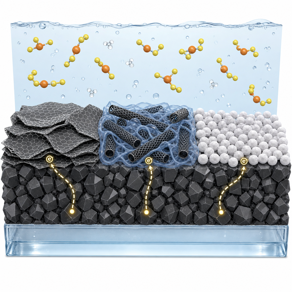
The ICIS absorber was deposited on FTO glass by nebulized spray pyrolysis from copper chloride, indium chloride, and thiourea precursors at 350 °C, yielding 1.2 µm thick, nanocrystalline, n-type films with a Hall mobility of 54 cm²/V·s. Graphene was synthesized by chemical reduction of graphene oxide (2 mg/mL Sigma-Aldrich dispersion) with dextrose and hydrazine hydrate, then sprayed onto the ICIS surface at 200 °C. To verify the quality of these in-house graphene layers, the authors referenced the technical data sheet for ACS Material Single Layer Graphene (Graphene Factory), comparing HRTEM lattice images and selected-area electron diffraction patterns. The observed multilayer crumpled-paper morphology and (002) d-spacing of 0.329 nm matched the commercial standard, confirming successful synthesis. SWCNT/PEDOT:PSS composites (0.35 wt/vol% SWCNT, sonicated then spin-coated at 2000 rpm) and ZnO quantum dots (2.9 nm diameter, synthesized from zinc acetate and KOH with CTAB surfactant) were prepared by parallel routes and similarly coated onto ICIS.
The three TCCR-coated electrodes were assembled with platinum counter electrodes in 1 M polysulfide electrolyte and characterized by EIS, photostability, and J-V measurements under 60–94 mW/cm² illumination. Graphene-coated ICIS extended the electron recombination lifetime to 100 ms versus 0.014 ms for the bare electrode—a roughly 10^4-fold improvement—and increased the electron diffusion length from 0.02 µm to 1.81 µm. The SWCNT/PEDOT:PSS composite, with a conductivity of 2.862 (Ω·cm)^-1 (more than three orders of magnitude above neat PEDOT:PSS), eliminated photocurrent decay entirely over 360 minutes, delivering a 95% stability gain over the unprotected electrode. ZnO quantum dots, with a blue-shifted 3.6 eV bandgap and antireflective behavior, produced the highest conversion efficiency at 0.024%, a 71% improvement over the 0.014% baseline. Charge-transfer resistances rose by a factor of 10 across all coated electrodes, confirming that the TCCR layers physically and electronically block recombination of photogenerated electrons with redox species in the electrolyte. The graphene films exhibited p-type conductivity, a Hall mobility of 221 cm²/V·s, and a carrier density of 1.98 × 10^16 cm^-3.
These results have direct implications for photoelectrochemical hydrogen production, dye-sensitized and quantum-dot-sensitized solar cells, and any chalcogenide-based solar absorber that operates in contact with a corrosive electrolyte. The demonstration that carbon nanostructures of different dimensionalities deliver complementary benefits—graphene for recombination suppression, SWCNT/PEDOT:PSS for hole extraction and long-term stability, and ZnO QDs for multiple exciton generation and antireflection—provides a design template for multilayer photoelectrodes. Follow-up work suggested by the authors includes tailoring the ICIS absorber's optoelectronic characteristics and combining the three TCCR strategies in a single hybrid stack to push photoconversion efficiency further while retaining the demonstrated chemical robustness.
For researchers building PEC cells, quantum-dot sensitized solar cells, or transparent-conductor stacks, having a reliable graphene reference is essential for distinguishing single-layer films from partially reduced graphene oxide. ACS Material's Single Layer Graphene, used here as the characterization benchmark, is available to laboratories working on similar passivation, transparent-electrode, and 2D heterostructure projects, along with the carboxyl, hydroxyl, and nitrogen-doped graphene variants needed for comparative interface engineering.How ACS Material products were used
- Single Layer Graphene (ACS Material Graphene Factory) (Graphene Series) — “Technical data sheet, Single layer Graphene, ACS Material Graphene factory, pg.no:3.”
Product Performance in this Study
The authors compared the structural features (HRTEM, SAED) of their chemically reduced graphene oxide film with the technical data sheet of ACS Material's Single Layer Graphene as a quality benchmark, confirming that their graphene layers matched the characteristics of the commercial standard.
Related product categories
Frequently asked questions
Why is graphene used as a passivation layer on CuInS2 photoelectrodes?
Graphene is one atom thick, optically transparent across the visible spectrum, and electrically conductive. When coated on CuInS2 in a photoelectrochemical cell, it forms a transparent conducting corrosion-resistant layer that blocks recombination between photogenerated electrons and redox species in the electrolyte. In this study, graphene increased the electron recombination lifetime by a factor of 10,000 and extended the electron diffusion length from 0.02 µm to 1.81 µm.
How does an SWCNT/PEDOT:PSS composite improve solar cell stability?
Single-walled carbon nanotubes bridge isolated conductive PEDOT islands across the insulating PSS phase, raising composite conductivity from 0.0027 to 2.862 (Ω·cm)^-1. The composite also acts as a hole-conducting layer that scavenges minority carriers from the photoelectrode. In this study, SWCNT/PEDOT:PSS coated CuInS2 showed essentially zero photocurrent decay over 360 minutes of illumination, a 95% stability improvement over the unprotected electrode.
Why do ZnO quantum dots boost the efficiency of CuInS2 photoelectrodes?
At 2.9 nm diameter, ZnO quantum dots exhibit strong quantum confinement, blue-shifting the bandgap to 3.6 eV and producing antireflective behavior on the electrode surface. They also support multiple exciton generation from single absorbed photons and offer high carrier mobility for efficient charge separation. In this work they delivered the highest conversion efficiency of all tested layers, a 71% improvement over the bare CuInS2 electrode.