-
Graphene/PbS QD NIR Photodetectors - KIMM, 2020
Jul 02, 2026 | ACS MATERIAL LLCJeong, H. et al. (2020). Graphene/PbS quantum dot hybrid structure for application in near-infrared photodetectors. *Scientific Reports*. https://doi.org/10.1038/s41598-020-69302-6
Scientific Reports · 2020
KIMM researchers combined ACS Material single-layer graphene with PbS quantum dots to build NIR photodetectors with 5x higher photocurrent and faster response.
About this research
Researchers at the Korea Institute of Machinery and Materials (KIMM) report a near-infrared photodetector built from a hybrid of ACS Material single-layer graphene and oleic-acid-capped PbS colloidal quantum dots, achieving roughly five-times higher photocurrent under 980-nm illumination compared with a PbS-only reference device. Published in Scientific Reports (2020) with co-authors from Sungkyunkwan University and the Korea University of Science and Technology, the work demonstrates that pairing a metallic 2D conductor with a tunable 0D semiconductor produces a thin, solution-processable photodetector that combines strong NIR absorption with fast carrier extraction.
Near-infrared photodetection is critical for telecommunications, biomedical imaging, night vision and gas sensing, yet incumbent crystalline semiconductors such as InGaAs are costly and difficult to integrate on flexible substrates. PbS colloidal quantum dots have emerged as a leading low-cost alternative because their direct band gap can be tuned across the short-wave infrared by simply controlling particle size. Pristine PbS QD films, however, suffer from slow inter-dot charge hopping that limits responsivity and response speed. Graphene complements PbS by providing a high-mobility transport channel and a work-function mismatch that drives photogenerated carriers out of the QDs. The challenge has been to form an intimate, processable graphene–QD interface without destroying either component, and to verify that charge transfer is actually occurring.
The graphene used in this study was supplied as single-layer graphene flakes from ACS Material, prepared by a modified Hummers method with average lateral diameters of 0.4–0.5 μm and thicknesses of 0.6–1.2 nm. The flakes were dispersed in hexane at 2 mg/mL and sonicated for 10 minutes together with PbS QDs whose first exciton peak sat at 950 nm. The resulting composite was drop-cast onto SiO2 substrates patterned with interdigitated 300-nm Au electrodes formed by photolithography and thermal evaporation. Ligand exchange of the PbS QDs with 1,2-ethanedithiol (EDT) was performed to shorten the inter-dot distance and improve carrier transport. Field-emission SEM and TEM imaging confirmed that the composite contained both aggregated and isolated single-layer flakes with characteristic wrinkles, decorated by close-packed, uniformly sized PbS QDs.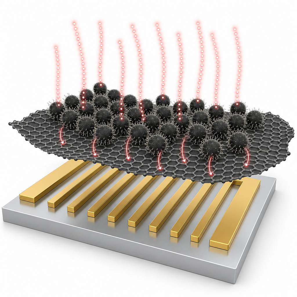
The optical and electrical characterization gives a consistent picture of strong, beneficial coupling. Absorbance of the graphene–PbS composite increased relative to either component alone, while photoluminescence from the PbS QDs was strongly quenched, indicating efficient non-radiative charge transfer to graphene. Raman spectroscopy under 633-nm excitation revealed enhancement of the PbS-specific vibrational mode embedded in the graphene spectrum, attributed to a surface-enhanced Raman scattering (SERS) chemical mechanism driven by photoinduced charge transfer between the two materials. Photocurrent measurements at 980 nm using a probe station showed that the graphene–PbS QD photodetector produced approximately five-times higher photocurrent than the PbS-only control device fabricated on the same electrode geometry. Dynamic response measurements demonstrated a 22% faster rise time and 47% faster decay time, both consistent with the addition of a fast graphene transport pathway that bypasses slow inter-dot hopping. Together these results validate the proposed device physics: PbS QDs harvest NIR photons, charge separates at the graphene/QD interface, and majority carriers traverse the graphene network to the Au electrodes.
The practical implications extend beyond laboratory photodetectors. Because the hybrid is solution-processable and atomically thin, it is well suited to flexible and transparent optoelectronics, including wearable health monitors, conformable imaging arrays, NIR security sensors and CMOS-compatible focal-plane arrays. The same architecture could be extended to short-wave infrared imaging by tuning PbS size, or coupled with plasmonic structures for narrowband detection. The authors point to flexible NIR photovoltaics, light-emitting devices and phototransistors as natural extensions of the graphene–PbS QD platform, all leveraging the same charge-transfer physics demonstrated here.
For researchers building 2D–0D hybrid devices, the consistency between the optical, vibrational and electrical evidence in this paper underscores the value of starting with well-characterized single-layer graphene. ACS Material's single-layer graphene and related graphene products are routinely used in photodetector, transistor and energy-storage research where flake thickness and lateral size directly determine device performance. Groups exploring NIR sensing, flexible electronics or SERS-based charge-transfer studies will find the same graphene grade a useful starting point for reproducing and extending this work.How ACS Material products were used
- Single Layer Graphene (Graphene Series) — “Single-layer graphene flakes (ACS Material) are fabricated using the modified Hummer's method. The average diameter and thickness of these graphene flakes ranged between 0.4–0.5 μm and 0.6–1.2 nm, respectively.”
Product Performance in this StudyThe single-layer graphene flakes were the conductive 2D component of the hybrid photodetector channel. Combined with PbS QDs, they enabled efficient photoinduced charge transfer, producing five-times higher photocurrent and 22%/47% faster rise/decay times than PbS-only devices.
Related product categories
Frequently asked questionsHow does single-layer graphene improve PbS quantum dot photodetectors?
Single-layer graphene provides a high-mobility transport channel that bypasses the slow inter-dot hopping limiting pure PbS quantum dot films. Because graphene and PbS have different work functions, photogenerated carriers separate at the interface and travel along the graphene to the electrodes. In this study the hybrid device produced about five-times higher photocurrent at 980 nm, with 22% faster rise and 47% faster decay times than a PbS-only reference.
What evidence confirms charge transfer between graphene and PbS quantum dots?
Three independent measurements support efficient charge transfer. The composite shows increased optical absorbance compared with each component alone. The strong photoluminescence of PbS quantum dots is quenched after mixing with graphene, indicating non-radiative depopulation of excited states. Raman spectroscopy reveals SERS-like enhancement of the PbS vibrational mode embedded in the graphene spectrum, which is attributed to the chemical enhancement mechanism driven by photoinduced charge transfer.
Why is single-layer graphene preferred over multilayer flakes for NIR photodetectors?
Single-layer graphene is atomically thin, optically transparent across the visible and near-infrared, and offers the highest carrier mobility per layer, all of which improve photodetector responsivity and speed without blocking incident light. The flakes used here were 0.6–1.2 nm thick and 0.4–0.5 μm wide, providing enough percolating pathways to extract carriers from the PbS quantum dot film while keeping the active layer flexible and transparent.