-
Graphene/Si Schottky 2 µm Photodetector — IMM-CNR, 2018
Jun 19, 2026 | ACS MATERIAL LLCCasalino, M. et al. (2018). Free-space schottky graphene/silicon photodetectors operating at 2 μm. *ACS Photonics*. https://doi.org/10.1021/acsphotonics.8b01037
Istituto per la Microelettronica e Microsistemi IMM-CNR, Via P. Castellino n. 111, 80131 Napoli, Italy · ACS Photonics · 2018
IMM-CNR built free-space graphene/silicon Schottky photodetectors operating at 2 µm using ACS Material monolayer graphene, reaching 10.3 mA/W internal responsivity.
About this research
Researchers at Istituto per la Microelettronica e Microsistemi IMM-CNR (Napoli, Italy), in collaboration with IRC-CNR and the University of Naples Federico II, used monolayer CVD graphene purchased from ACS Material to fabricate free-space-illuminated Schottky graphene/silicon photodetectors operating at 2 µm at room temperature. The devices achieved an internal responsivity of 10.3 mA/W (external 0.16 mA/W) at 2 µm, in close agreement with internal photoemission theory based on the extracted Schottky barrier. The work demonstrates a simple, Si-CMOS-compatible route to photodetection beyond germanium's cutoff wavelength.
The 2 µm wavelength window is of growing importance for silicon photonics. Two-photon absorption, which limits nonlinear processes near 1.55 µm, effectively vanishes; silicon-on-insulator waveguides still confine light efficiently; and several gas absorption lines, including CO2, sit close to 2 µm, opening applications in chemical and biological sensing, environmental monitoring, free-space optical communication, optical coherence tomography (OCT), and light-radar (LiDAR). However, silicon's 1.12 eV bandgap blocks direct band-to-band detection beyond ~1.1 µm, and germanium-on-silicon detectors lose responsivity above ~1.6 µm. Defect-mediated and ion-implanted silicon photodiodes have been demonstrated at 2–2.5 µm but require implantation and annealing steps. A graphene/silicon Schottky junction offers an alternative based on internal photoemission, where photons absorbed in graphene excite carriers that surmount the Schottky barrier into silicon, circumventing the silicon bandgap.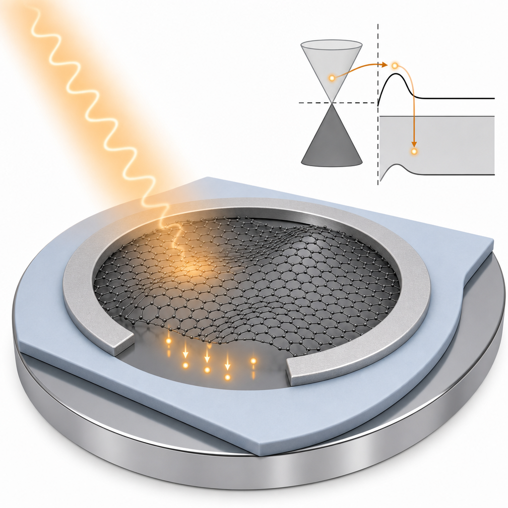
The ACS Material CVD graphene was delivered as a monolayer protected by a 500 nm PMMA layer on a polymer carrier, ready for wet transfer. The authors prepared a low-doped (~10^15 cm^-3) p-type silicon substrate with a thermal SiO2 mask, defined an Al ohmic ring contact and Cr/Au pads, and opened a 50 µm-diameter window for the Schottky contact. Just prior to graphene transfer, residual native oxide was removed in dilute HF (2%) for 1 minute. The PMMA-graphene film was released onto deionized water, scooped onto the chip, dried, baked, and the PMMA was dissolved in acetone. O2 plasma etching then patterned a graphene disk surrounded by the Al ohmic ring. Raman spectroscopy on the transferred film (532 nm excitation, 100× objective) showed a single-Lorentzian 2D peak at 2683 cm^-1, no measurable D peak, a G peak at 1586 cm^-1, and I(2D)/I(G) ≈ 2.5, confirming high-quality, single-layer, lightly-doped graphene suitable for the device's active interface.
Electrical characterization between 280 K and 315 K revealed a clearly rectifying junction with a reverse dark current of about 8 nA at -1 V versus 3.5 µA forward current at +1 V — more than two orders of magnitude difference. Fitting the I–V data with thermionic emission yielded a Schottky barrier of 0.621 ± 0.004 eV at 300 K and zero bias, in good agreement with the theoretical value of 0.67 eV calculated from a graphene workfunction of 4.5 eV. The barrier height showed a linear dependence on inverse temperature, consistent with a Gaussian distribution of barrier inhomogeneities (mean SBH = 1.018 eV, σ = 0.143 eV) arising from corrugations and electron-density variations in the transferred graphene. Conductance-frequency measurements with an LCZ meter extracted an interface trap capacitance Cit = 1.75 × 10^-5 F/cm^2, a trap lifetime of 2 ms, and an interfacial trap density of 1.1 × 10^14 eV^-1cm^-2 — higher than for standard SiO2/Si interfaces, indicating dangling bonds and charge traps that pin the Fermi level. Optoelectronic measurements used a 2 µm diode laser (Thorlabs FPL2000S), a beam splitter, and a calibrated InGaAs reference detector, with photocurrent read by a lock-in amplifier. The photocurrent scaled linearly with absorbed optical power; using a calculated single-layer graphene absorptance of 1.579% at 2 µm, the internal responsivity reached 10.3 mA/W, while the external responsivity was 0.16 mA/W.
The demonstrated performance is competitive with implanted silicon photodiodes at 2 µm (3–10 mA/W) but without ion-implantation steps, making the architecture attractive for low-cost integration with silicon photonic circuits. Free-space-illuminated Schottky graphene/Si detectors of this type can serve as building blocks for 2 µm free-space optical communication links, OCT systems, gas sensors targeting the CO2 absorption window near 2 µm, and LiDAR receivers. The detailed characterization of interfacial trap density and barrier inhomogeneity also gives a clear engineering path: reducing transfer-induced corrugations and dangling-bond density should raise both barrier uniformity and responsivity.
For researchers pursuing mid-infrared silicon photonics, the study underscores the value of high-quality monolayer CVD graphene as a Schottky junction material. The PMMA-coated CVD graphene on copper or polymer carriers offered by ACS Material — the same product family used here — is directly applicable to similar Schottky photodetectors, transparent electrodes, and 2D-material-based optoelectronic devices, and is available in the CVD Graphene product line for groups working on 2 µm photodetection, IR sensing, and Si-photonic integration.How ACS Material products were used
- CVD Graphene (monolayer, PMMA-coated on polymer substrate for wet transfer) (CVD Graphene) — “Graphene was purchased from ACS Material [41]. The upper side of the graphene monolayer is covered with 500 nm of PMMA and the PMMA-graphene film is laid on a polymer substrate.”
Product Performance in this StudyThe ACS Material monolayer graphene formed the Schottky contact with p-Si and served as the photoactive absorber at 2 µm. Raman analysis confirmed single-layer character with negligible defects (no D peak) and negligible doping (I(2D)/I(G)≈2.5), and the device delivered an internal responsivity of 10.3 mA/W in good agreement with theory.
Related product categories
Frequently asked questionsWhy use graphene instead of germanium for silicon-based 2 µm photodetectors?
Germanium-on-silicon photodetectors lose responsivity above ~1.6 µm because of germanium's cutoff wavelength, which makes them unsuitable at 2 µm. A graphene/silicon Schottky junction detects via internal photoemission: photons absorbed in graphene excite carriers that surmount the Schottky barrier into silicon. This mechanism is wavelength-flexible and bypasses the silicon bandgap, making graphene a strong candidate for 2 µm operation while remaining CMOS-compatible.
What internal responsivity can a graphene/silicon Schottky photodetector reach at 2 µm?
The IMM-CNR device demonstrated an internal responsivity of 10.3 mA/W and an external responsivity of 0.16 mA/W at 2 µm under room-temperature, free-space illumination. These values agree well with internal photoemission theory using the measured Schottky barrier height of 0.621 eV and a calculated single-layer graphene absorptance of 1.579%, and are competitive with reported ion-implanted silicon photodiodes operating in the same wavelength window.
How is monolayer CVD graphene transferred onto a silicon Schottky photodetector?
The CVD graphene from ACS Material is supplied with a 500 nm PMMA protective layer on a polymer carrier. After removing residual native oxide on silicon with dilute HF, the PMMA-graphene film is released onto deionized water, scooped up by the patterned chip, dried with nitrogen, baked on a hot plate, and the PMMA is dissolved in acetone. Photolithography and O2 plasma etching then define the active graphene disk on the silicon Schottky window.