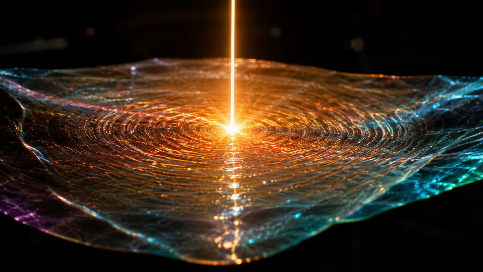
When graphene arrived, the established thermal toolbox struggled to hold it: an atom-thick membrane offers no disc to flash, no plane to clamp, no easy surface for a heater line — conventional bulk and contact-based architectures were poorly suited to the geometry. Optothermal Raman thermometry solved the impasse with a beautiful inversion — let the laser that probes the crystal also heat it, and read the temperature from the crystal’s own vibrational spectrum, since Raman peaks slide measurably with temperature. The first suspended-graphene measurements built on exactly this idea produced the celebrated ultrahigh room-temperature conductivities that launched a field1. They also launched a decade of spirited disagreement, because the method’s most important input — how much laser power the atomic layer actually absorbed — was the hardest to measure23. This article explains both halves honestly: the elegance, and the error budget.
- 1The inversion: probe as heater, spectrum as thermometer
- 2What it delivered: the 2D thermal field’s founding numbers
- 3The error budget, ingredient by ingredient
- 4Interactive: propagate the uncertainties yourself
- 5Supported crystals: measuring the state that ships
- 6Cross-checking with the electrothermal family
- 7Raman thermometry in the method landscape
- 8Frequently asked questions
- 9Keep exploring the knowledge hub
- 10References
The inversion: probe as heater, spectrum as thermometer
Raman scattering already reports on a crystal’s phonons; temperature softens those phonons, sliding characteristic peaks — graphene’s G and 2D bands among the best studied — by a calibratable rate of order a few hundredths of a wavenumber per kelvin1. Optothermal Raman weaponizes the coincidence: increase the laser power, watch the peak slide, and you have measured the temperature rise at the focal spot with no contact whatsoever. Suspend the crystal over a hole or trench so heat must flow radially through the layer itself to the supported rim, and the ratio of absorbed power to temperature rise, through the appropriate conduction geometry, is the layer’s thermal conductivity12.
The architecture’s virtues are real and specific: no heater or thermometer fabricated on the crystal itself (transfer and suspension preparation remain real work), micrometer spatial selectivity, chemical specificity for free (the same spectrum identifies layer number and strain), applicability across the 2D family and its heterostructures4, and applicability to exactly the suspended-membrane geometry no clamp or disc method can touch2.
What it delivered: the 2D thermal field’s founding numbers
The founding measurement reported suspended single-layer graphene in the several-thousand W m⁻¹K⁻¹ class at room temperature — above natural diamond — and made 2D thermal transport a field overnight1. Refinements followed rapidly: measuring the transmitted and reflected beam to constrain absorption directly, CVD-grown membranes extending the geometry, and supported-graphene measurements quantifying how substrate contact suppresses the conductivity relative to suspension — the number engineering actually inherits235. Independent electrothermal work on giant CVD sheets corroborated the class of values by an entirely different signal path36 — consistent in magnitude, though on different specimens with different support states and defect populations, so strict same-sample corroboration remains the harder, rarer experiment.
The error budget, ingredient by ingredient
Absorbed power — the historical dominator. The conductivity scales directly with how much of the incident beam the layer absorbed, and for an atomically thin crystal that fraction is small, wavelength-dependent, contamination-sensitive, and — in the early era — often taken from theory rather than measured. Differences in assumed absorbance alone account for a substantial part of the early literature’s spread; modern practice measures transmission and reflection on the same membrane2.
Peak-shift thermometry. The temperature-rise uncertainty is itself a composite: the Raman temperature coefficient’s calibration, peak-position estimation to a small fraction of a wavenumber under deliberately varied power, the local-heating model, and — at the frontier — optical–acoustic phonon non-equilibrium all contribute as distinct terms in the budget1. Strain and doping shift the same peaks, demanding that only temperature vary across the power series.
Geometry and model form. The radial-conduction model assumes the suspended region’s boundary sits at the rim temperature and the spot profile is known; hole size, spot size and rim contact all enter, and interfacial conductance at the rim is its own subject7. None of these is fatal; all belong in the stated budget, per the standard uncertainty frameworks89.
Interactive: propagate the uncertainties yourself
The simulator applies first-order propagation to the two leading ingredients — absorbed-power uncertainty and combined temperature-rise uncertainty — and reports the conductivity error bar they alone justify. Set the dials to the early era’s assumed-absorbance conditions and the celebrated spread of published values stops looking mysterious.
Supported crystals: measuring the state that ships
Devices do not use suspended membranes; they use crystals on substrates, where phonon leakage and interface scattering suppress the in-plane conductivity well below the suspended ceiling — the supported-graphene measurements made that suppression quantitative and permanent5. The engineering consequence threads through this hub: the number that matters for a heat-spreading film10 or a supported device layer is the supported-state number, measured in a geometry faithful to the application — the exact philosophy behind the supported-composite electrothermal protocols for 2D materials1112.
Cross-checking with the electrothermal family
Raman thermometry and the suspended electrothermal family are natural cross-checks because their signal-generation and thermometry chains are largely independent: optical versus electrical signal paths, spot heating versus distributed Joule heating, spectral versus resistive thermometry. Where both can hold a sample class — supported and free-standing 2D layers, thin films on membranes — agreement between them provides a strong independent cross-check and reduces the plausibility of dominant uncorrelated biases — while shared assumptions (geometry, support effects, thickness definitions, sample non-uniformity) can still bias both routes in the same direction311. The electrothermal side brings its own ledger — measured resistance and power in, contact and coating corrections out, audited by differential designs1314 — and modern TET variants even inherit Raman’s laser as a heater while keeping resistive readout, trading the absorbance problem for a calibration one1516. Analogous residual, fit-window and uncertainty checks apply to both families, although their governing models and error structures are not identical1718.
Raman thermometry in the method landscape
| Question | Optothermal Raman1 | Supported-differential TET11 | Micro-bridge19 | TDTR20 |
|---|---|---|---|---|
| Native 2D geometry | Suspended membrane over hole | Sheet on support membrane | Flake across two membranes | Supported film under transducer |
| Thermometer | Raman peak shift | Sample resistance | Pt resistance on device19 | Thermoreflectance21 |
| Dominant systematic | Absorbed power23 | Support subtraction share12 | Background + contacts7 | k–G correlation22 |
| Fabrication on sample | None | Transfer to support | Placement on device | Sputtered transducer |
| Chemical specificity | Built-in (same spectrum) | No | No | No |
Frequently asked questions
Why did early graphene conductivity values disagree so widely?
Mostly the absorbed-power input: assumed versus measured absorbance differed enough to move the answer by large factors, with thermometry calibration and geometry contributing the rest. As laboratories measured absorption on the same membrane and stated full budgets, the spread narrowed — the method matured rather than failed238.
Is the suspended-graphene number the one I should design with?
Only if your application suspends graphene. Supported and encased layers conduct substantially less, and composite architectures less again — design values should come from measurements in the application-faithful state, which is exactly what supported-state protocols exist to provide511.
Does Raman thermometry work on materials other than graphene?
A crystal qualifies when several conditions hold together: a peak with sufficient temperature sensitivity, determinable absorbed power, modelable geometry and boundaries, tolerable photodamage thresholds, and controlled optical–acoustic phonon non-equilibrium. Transition-metal dichalcogenides prominently qualify; the error discipline travels with the method2.
Keep Exploring the ACS Thermal Metrology Knowledge Hub
This article is one chapter of the ACS thermal metrology knowledge hub. To keep going:
- Thermal conductivity & diffusivity testing: the pillar guide — the full landscape in one place.
- Differential TET for 2D materials — the electrothermal cross-check in its supported-state geometry.
- TPET: laser-heated electrothermal characterization — Raman’s heater, TET’s thermometer.
- Which thermal measurement method should you use? — the interactive decision hub.
- Graphene Series materials — the crystals these methods were built to measure.
References
This article describes optothermal Raman thermometry and its comparison with electrothermal approaches for educational purposes. The interactive model is a simplified first-order uncertainty propagation, not a full metrological budget. For sample-specific feasibility and formal quotes, contact our thermal testing team.