-
Silver Nanowire Transparent Electrodes - ÉTS Montréal, 2021
Jul 02, 2026 | ACS MATERIAL LLCGerlein, L., Benavides-Guerrero, J., & Cloutier, S. (2021). High-performance silver nanowires transparent conductive electrodes fabricated using manufacturing-ready high-speed photonic sinterization solutions. *Scientific Reports*.
Scientific Reports · 2021
ÉTS Montréal team uses ACS Material silver nanowires and photonic curing to make transparent electrodes with 88.3% T and 9.8 Ω/sq, outperforming ITO by 2.6-2.7×.
About this research
Researchers at École de technologie supérieure (Montréal) demonstrated that silver nanowires purchased from ACS Material, deposited by dip-coating and processed with high-speed photonic sintering on a Novacentrix PulseForge Invent system, produce transparent conductive electrodes (TCEs) that outperform commercial indium tin oxide (ITO) by a factor of 2.6-2.7× across two standard figures-of-merit. The champion two-layer electrode reaches an optical transmittance of 88.3% in the visible range and a sheet resistance of just 9.8 Ω/sq, comparable to thermally annealed silver nanowire films but produced in milliseconds on substrates that cannot tolerate conventional 300 °C annealing. The result establishes a manufacturing-ready route to TCEs for flexible hybrid electronics.
Transparent conductive electrodes are essential to solar cells, OLED displays, touch panels, wearable sensors and biomedical devices. ITO dominates the market but is brittle, supply-constrained and ill-suited to roll-to-roll production on plastic. Doped metal oxides such as AZO and FTO inherit similar manufacturing limitations, while conductive polymers like PEDOT:PSS suffer from oxidation and photodegradation. Randomly distributed metallic nanowire meshes have emerged as the most credible ITO alternative because they combine low sheet resistance, high transmittance and bending tolerance. Yet they normally require thermal annealing above 300 °C or slow laser scanning to weld nanowire junctions, which conflicts with both low-temperature substrates and high-throughput manufacturing. The open question this paper addresses is whether intense pulsed-light (photonic) sintering can deliver ITO-beating performance at line speeds compatible with industrial printed electronics.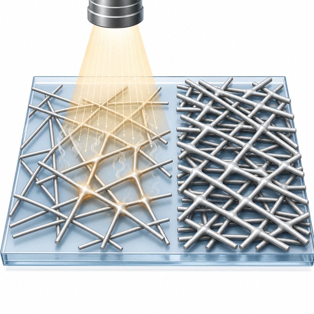
The ACS Material silver nanowire product is described in the Methods section as "a dispersion of silver nanowires in ethanol... purchased from ACS material chemical supplier" with an average nanowire diameter of 120 nm and lengths of 20-30 µm. The authors adjusted the as-received dispersion to 10 mg/mL and used it directly without further purification. Glass substrates were cleaned with detergent and sequential isopropanol/acetone sonication, then dip-coated with a 5 s immersion still time and 200 mm/min withdrawal velocity. Repeated dip-coating cycles produced one, two, three, four or five nanowire layers, allowing density to be tuned against transparency. Each sample was photonically sintered with 15 consecutive 30,000 µs pulses at 24.5 J cm-2 fluence, calibrated using Novacentrix SimPulse simulations to bring the film to ~300 °C while keeping the underlying glass cool enough to avoid damage. Commercial silver-flake paste was drop-cast at the corners for electrical contacts.
The optical and electrical performance scaled cleanly with nanowire density. Visible-range transmittance averaged 91.5%, 88.3%, 82.8% and 74.7% for one, two, three and four layers, while sheet resistance dropped from 15.3 Ω/sq (one layer) to 9.8, 6.1, 5.4 and 3.0 Ω/sq for two through five layers. Surface fill factor rose from 16.4% (one layer) to 28.8% (four layers). The two-layer electrode emerged as the champion device, balancing 88.3% transmittance against 9.8 Ω/sq sheet resistance with a non-uniformity factor of 26%. Using the De et al. electrical-to-optical conductivity figure-of-merit, this corresponds to σDC/σOP = 317 Ω-1, versus 118.7 Ω-1 for standard ITO-on-glass at 90.2% transmittance and 30 Ω/sq - a 2.67× improvement. Using Haacke's transparent-conductor figure-of-merit, the same sample achieves φTC = 0.031 Ω-1 compared with 0.012 Ω-1 for ITO, a 2.58× gain. SEM imaging before and after photonic curing confirmed that the pulsed light removed the residual PVP surfactant from the nanowires and welded the junctions through plasmon-resonance heating without spheroidizing the wires. Haze remained near 16% before and after treatment, an acceptable level for photovoltaic windows. The authors also introduced a new pulse-fluence-based figure-of-merit (φPT) and identified an optimum at 26.4 J cm-2, beyond which light-induced damage degrades conductivity.
Because photonic sintering equilibrates film and substrate temperatures within milliseconds, the process is compatible with polyethylene terephthalate, polyimide and other low-temperature flexible substrates. This makes the demonstrated electrodes immediately relevant to printed organic photovoltaics, flexible OLED lighting and displays, capacitive touch sensors, wearable strain and pressure sensors, electrochromic windows and biomedical electrodes. The compatibility with PulseForge industrial pulse engines means the recipe can in principle be transferred to roll-to-roll lines without redesign. The authors point to further work on Meyer-rod or dynamic-heating deposition to reduce the 26% non-uniformity, and on extending the photonic curing protocol to copper, nickel and hybrid graphene/nanowire architectures.
For researchers and process engineers developing the next generation of flexible transparent electrodes, the ACS Material silver nanowire dispersion (120 nm diameter, 20-30 µm length) used in this study is available from ACS Material's Nanowire Series. The combination of well-controlled nanowire geometry and ethanol-based dispersion supported reproducible dip-coating and clean photonic welding, which together underpinned the ITO-beating figures-of-merit reported here. The product is suited to groups exploring printed photovoltaics, flexible displays, transparent heaters and wearable sensor electrodes where ITO is impractical.How ACS Material products were used
- Silver Nanowires Dispersion in Ethanol (120 nm diameter, 20-30 µm length) (Nanowire Series) — “A dispersion of silver nanowires in ethanol is purchased from ACS material chemical supplier. The average nanowire diameter is 120 nm and their lengths range from 20 to 30 µm.”
Product Performance in this StudyThe ACS Material silver nanowires were the core conductive material forming the transparent electrode mesh. After optimized photonic sintering, two layers delivered 88.3% transparency and 9.8 Ω/sq sheet resistance, yielding 2.6-2.7× higher figures-of-merit than commercial ITO.
Related product categories
Frequently asked questionsHow does photonic sintering improve silver nanowire transparent electrodes?
Photonic sintering uses millisecond-scale broadband light pulses to excite plasmon resonance in silver nanowires, locally heating their junctions to about 300 °C while keeping the substrate cool. This welds nanowire crossings into a continuous conductive network and removes residual PVP surfactant, dropping sheet resistance to single-digit Ω/sq without damaging plastic substrates - something conventional thermal annealing cannot achieve on flexible films.
What sheet resistance and transmittance can silver nanowire electrodes achieve compared with ITO?
In this study, a two-layer dip-coated silver nanowire electrode reached 88.3% visible-range transmittance and 9.8 Ω/sq sheet resistance after photonic sintering. Commercial ITO-on-glass typically shows 90.2% transmittance at 30 Ω/sq. Using the De et al. figure-of-merit, this corresponds to σDC/σOP = 317 Ω-1 versus 118.7 Ω-1 for ITO, a 2.67× improvement at comparable transparency.
What silver nanowire dimensions are best for transparent conductive electrodes?
The authors used 120 nm diameter silver nanowires with 20-30 µm length dispersed in ethanol at 10 mg/mL. This aspect ratio supports percolation at low coverage, preserving transmittance above 88% while allowing efficient plasmonic absorption of pulsed-light energy at the nanowire junctions. Thinner wires reduce haze but raise sheet resistance, so dimensions should be matched to the target application's optical and electrical specifications.