-
Silver Nanowire–Graphene Electrodes for OSCs — James Cook University, 2023
Jun 26, 2026 | ACS MATERIAL LLCKamel, M., & Stoppiello, C. (2023). Improved transfer-free sustainable graphene electrode using silver nanowires for organic photovoltaics. *ACS Applied Energy Materials*. https://doi.org/10.1021/acsaem.3c02001
ACS Applied Energy Materials · 2023
James Cook University researchers combined ACS Material silver nanowires with transfer-free PECVD graphene, reaching 9.75% PCE in ITO-free organic solar cells.
About this research
James Cook University researchers, working with collaborators at The University of Queensland, used silver nanowire (AgNW) dispersion purchased from ACS Material to engineer a transfer-free hybrid transparent conductive electrode (TCE) for organic solar cells, reaching a power conversion efficiency of 9.75% with a PM6:Y6 active layer — comparable to the 10.3% obtained on commercial ITO. The work, published in ACS Applied Energy Materials in 2023, demonstrates that pairing spin-coated AgNW networks with plasma-CVD graphene grown directly on glass eliminates the lossy graphene transfer step that has historically held back ITO-free photovoltaic electrodes.
Transparent conductors are a quiet bottleneck in next-generation photovoltaics. Indium tin oxide dominates the market but is brittle, indium-scarce, and incompatible with flexible substrates. Graphene is the obvious alternative — atomically thin, mechanically robust, chemically stable — yet single-layer graphene's sheet resistance is too high for practical electrodes, and chemical doping degrades both transmittance and stability. AgNW hybridization is a promising fix, but most prior demonstrations relied on CVD graphene grown on copper and then wet-transferred onto AgNW-coated glass, a process that introduces contamination, tears, and cost. The James Cook team set out to combine AgNWs with graphene grown directly on the device substrate from a sustainable plant-derived carbon source, eliminating transfer entirely.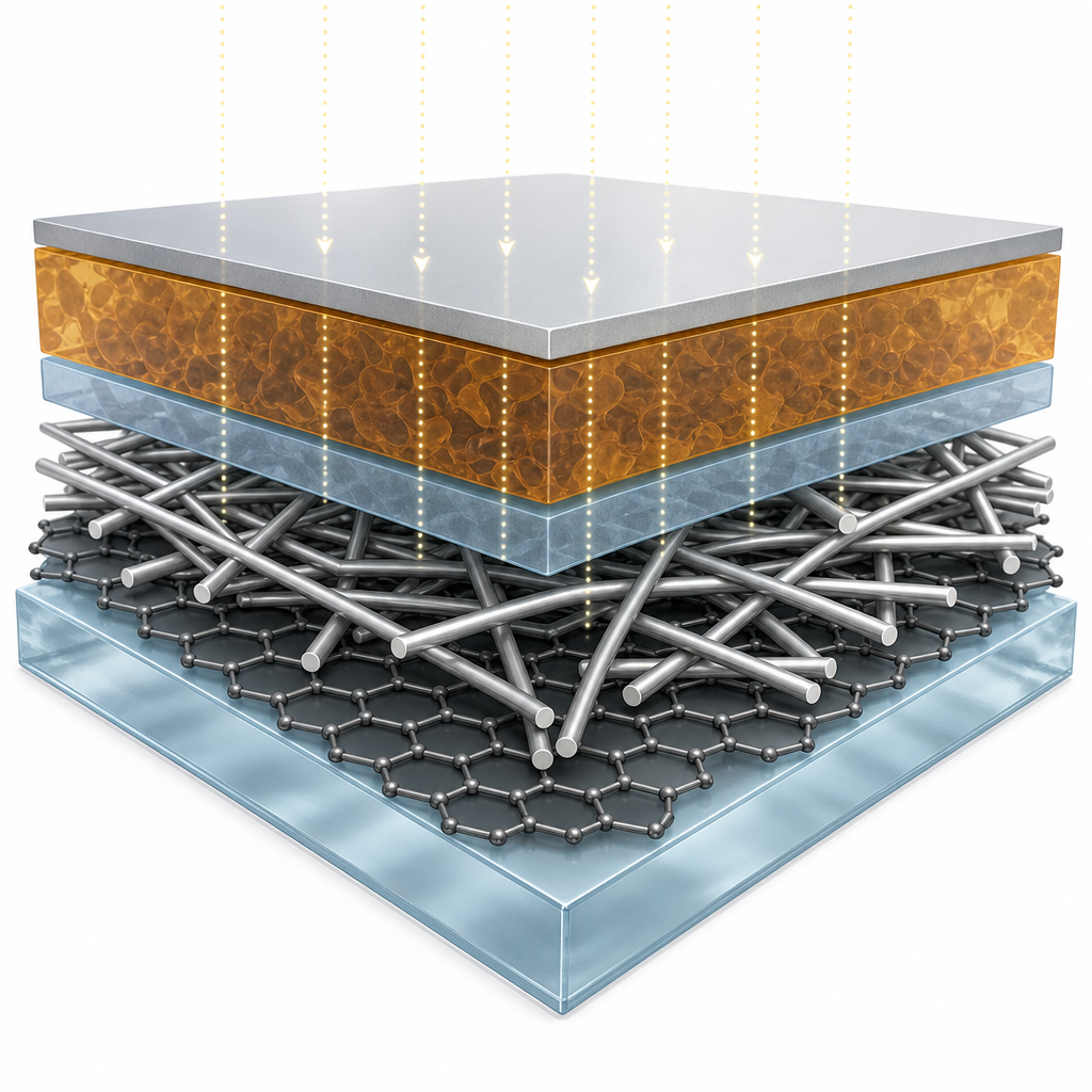
The ACS Material AgNW product — supplied as a 20 mg/mL dispersion in isopropyl alcohol with average nanowire diameter of 40 nm, length of 20–60 µm, and 99.5% purity — was diluted with IPA to working concentrations of 1, 2, and 3 mg/mL. The diluted dispersion was shaken, allowed to stabilize for 30 minutes, and spin-coated at 3000 rpm for 60 s onto oxygen-plasma-treated glass. Two electrode architectures were studied: AgNWs-Gr, where the nanowire network was laid down first and graphene was deposited on top using RF-PECVD at 600 °C from Pelargonium graveolens (geranium oil) vapor; and Gr-AgNWs, where the same plant-derived graphene was synthesized first and AgNWs were spin-coated on top. The Gr-AgNWs geometry proved more effective because graphene deposition at 600 °C degraded the underlying nanowire network in the AgNWs-Gr stack, an effect that limited improvement at higher AgNW loadings.
Quantitatively, pristine PECVD graphene exhibited a sheet resistance (Rs) of 1.92 kΩ/□ with 73.3% optical transmittance. Adding a 1 mg/mL AgNW spin-coat on top lowered Rs to 1.26 kΩ/□ while keeping transmittance essentially unchanged at 73%. Increasing the AgNW concentration to 3 mg/mL drove Rs down to 103 Ω/□ with transmittance still at 66%. Inverted organic solar cells with the structure TCE/ZnO/active layer/MoO3/Ag were then fabricated. P3HT:PCBM devices on pristine graphene gave a PCE of 1.41% and fill factor (FF) of 0.47; on Gr-AgNWs-1 the PCE rose to 1.85% with FF of 0.61, and on Gr-AgNWs-3 to 2.18% with FF of 0.63 — closely tracking the ITO control's 2.22% PCE and 0.60 FF. The high-performance PM6:Y6 system on the Gr-AgNWs hybrid reached 9.75% PCE versus 10.3% on ITO. The reverse AgNWs-Gr architecture peaked at 1.56% PCE for the 1 mg/mL loading and degraded at 3 mg/mL (1.13% PCE) due to non-uniform graphene growth on the nanowire network.
The demonstration matters for several adjacent application spaces. Most directly, it provides a route to ITO-free, transfer-free, and indium-free photovoltaic electrodes using a plant-extract carbon precursor — a meaningful step toward sustainable OPV manufacturing. The same hybrid TCE concept is applicable to flexible OLEDs, electrochromic windows, transparent heaters, touch panels, and wearable sensor backplanes where ITO's brittleness is a known failure mode. The authors note that lowering the graphene deposition temperature below 600 °C should preserve the AgNW network in the AgNWs-Gr architecture and likely unlock further performance gains, pointing to roll-to-roll-compatible processing on plastic substrates as a next step.
For researchers working on transparent electrodes, organic photovoltaics, or flexible optoelectronics, the silver nanowire dispersion used here is available from ACS Material in the Nanowire Series. The product's well-defined diameter, high aspect ratio, and IPA carrier solvent make it directly compatible with spin coating, spray coating, and Mayer-rod processes — the same toolkit being used across the TCE community. Pairing it with PECVD or CVD graphene films, or with other 2D conductive layers, is a reproducible recipe for low-sheet-resistance, high-transparency electrodes without resorting to indium.How ACS Material products were used
- Silver Nanowire dispersion in IPA (20 mg/mL, ~40 nm diameter, 20–60 µm length, 99.5% purity) (Nanowire Series) — “AgNWs dispersion in isopropyl alcohol (IPA) with a concentration of 20 mg/ml was purchased from ACS Material with an average diameter 40 nm, length of 20 – 60 µm, and purity of 99.5%.”
Product Performance in this StudyThe ACS Material AgNW dispersion provided the conductive nanowire networks combined with PECVD-grown graphene to form transfer-free hybrid transparent conductive electrodes. The AgNWs bridged graphene domains, lowering sheet resistance from 1.92 kΩ/□ to 103 Ω/□ in the best configuration while maintaining usable optical transmittance and enabling OSC PCEs comparable to ITO.
Related product categories
Frequently asked questionsHow do silver nanowires improve transfer-free graphene electrodes for solar cells?
Silver nanowires spin-coated onto transfer-free PECVD graphene act as additional conducting channels that bridge neighboring graphene domains. In this James Cook University study, adding ACS Material AgNWs lowered sheet resistance from 1.92 kΩ/□ to as low as 103 Ω/□ while maintaining 66–73% optical transmittance. The improvement enabled inverted organic solar cells whose power conversion efficiency closely matched ITO-based control devices, without requiring a wet graphene transfer step.
What silver nanowire dimensions are best for transparent conductive electrode research?
For TCE applications, AgNWs with diameters of roughly 30–50 nm and lengths of tens of micrometers strike the right balance between conductivity and transparency. The dispersion used in this paper was 40 nm in diameter and 20–60 µm in length, supplied at 20 mg/mL in isopropyl alcohol at 99.5% purity. Higher aspect ratios reduce the number of resistive nanowire junctions needed for percolation, allowing thinner networks that remain optically transparent.
Why deposit graphene after silver nanowires instead of transferring it on top?
Wet transfer of CVD graphene onto AgNW networks introduces polymer residues, tears, and contamination that degrade conductivity and yield. Direct PECVD growth of graphene from a plant-extract carbon source on AgNW-coated substrates eliminates these issues, but the 600 °C deposition temperature can damage the nanowires. This study found the reverse architecture — graphene first, AgNWs spin-coated on top — outperformed both alternatives, reaching 9.75% PCE with PM6:Y6 active layers.