-
Silver Nanowire/Graphene Transparent Electrodes for OPV - Hanyang University, 2017
Jun 29, 2026 | ACS MATERIAL LLCCamic, B. T. et al. (2017). Fabrication of a transparent conducting electrode based on graphene/Silver nanowires via layer-by-Layer method for organic photovoltaic devices. *Journal of Colloid and Interface Science*. https://doi.org/10.1016/j.jcis.2017.05.065
Journal of Colloid and Interface Science · 2017
Researchers built ITO-free transparent electrodes by layer-by-layer assembly of graphene oxide and ACS Material silver nanowires for organic solar cells.
About this research
Researchers at Hanyang University, working with collaborators at Yildiz Technical University, used silver nanowires supplied by ACS Material to construct a graphene/silver nanowire (G/Ag NW) transparent conducting electrode (TCE) via layer-by-layer (LBL) assembly, and integrated this hybrid film as the front electrode in P3HT:PCBM organic photovoltaic (OPV) devices. The work, published in the Journal of Colloid and Interface Science in 2017, demonstrates a fully solution-processable route to indium tin oxide (ITO)-free transparent electrodes. The approach combines amine-functionalized Ag NWs with graphene oxide (GO) sheets through electrostatic self-assembly and uses NaBH4 reduction plus thermal annealing to convert the GO/Ag NW stack into a conductive G/Ag NW hybrid film.
Transparent conducting electrodes are the gating cost and supply-chain bottleneck for organic solar cells, OLEDs, and flexible touch panels. ITO dominates the market but suffers from indium scarcity, brittleness on flexible substrates, and high-temperature sputter processing that is incompatible with polymer foils. Silver nanowire networks and graphene films are both leading ITO alternatives, yet each has weaknesses: bare Ag NW networks suffer from high wire-to-wire junction resistance and poor adhesion, while CVD or solution-cast graphene films have lower in-plane conductivity than metallic films at comparable transmittance. Hybridizing the two materials is a well-motivated strategy, but only if a scalable, low-temperature assembly route can be found. This paper addresses that need with a glass-substrate-compatible LBL process.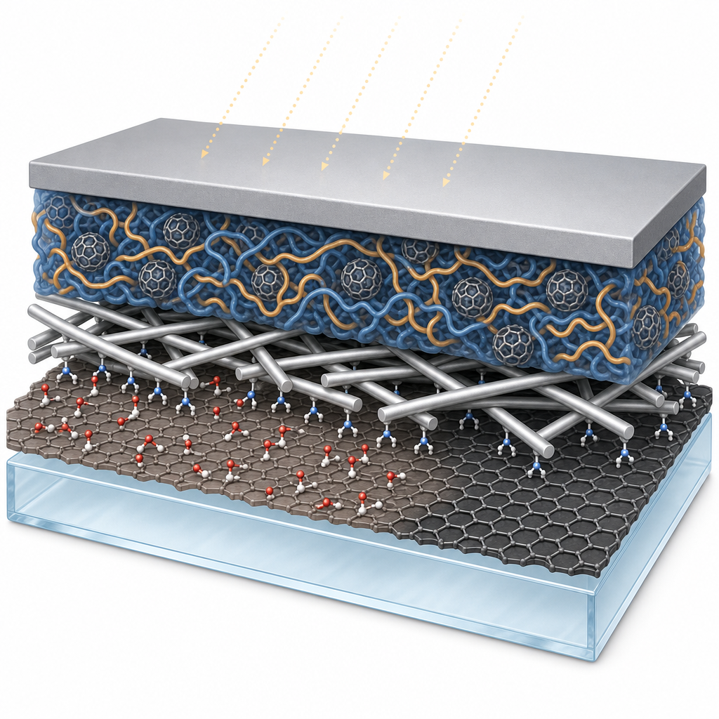
The ACS Material silver nanowires were specified as 50 nm average diameter, 5-10 µm length, dispersed in isopropanol at 20 mg/mL - a geometry that supports high optical transmittance with sparse percolating networks. The authors first surface-modified these Ag NWs with cysteamine (HSCH2CH2NH2) via a ligand exchange in which the thiol bonds to surface silver, leaving a protonated amine tail exposed. XPS confirmed S-Ag, S-H, and S-C peaks at 162.3, 163.3, and 164.4 eV respectively, and zeta-potential measurements gave +31.2 mV for the modified Ag NWs-NH2 versus -40.8 mV for GO at pH 10. APTES-functionalized glass substrates were spin-coated with GO (1 mg/mL, 150 µL, 2500 rpm) and then dip-coated for 20 minutes in the cationic Ag NWs-NH2 dispersion (0.5 mg/mL). Repeated cycles built up multilayer GO/Ag NW films, which were then reduced in 150 mM NaBH4 for 2 h and annealed in a tube furnace at 230 °C for 30 minutes.
The characterization confirmed that the LBL process produced uniform hybrid films with the Ag NW network embedded in reduced graphene oxide sheets. Raman spectroscopy of the GO showed the expected G band near 1580 cm-1 and D band near 1350 cm-1. Optical microscopy, AFM and FE-SEM showed Ag NWs anchored across the rGO underlayer rather than aggregating, which the authors attribute to the strong electrostatic interaction between the +31 mV Ag NWs-NH2 and the highly negative GO surface. Four-point-probe measurements on the LBL G/Ag NW films gave sheet resistance values low enough to operate as the transparent front contact in a working OPV cell, with optical transmittance in the visible range comparable to commercial ITO-coated glass. P3HT:PCBM bulk heterojunction devices were built directly on the G/Ag NW substrate using V2O5 as the hole transport layer and a 100 nm aluminum top electrode, and J-V curves recorded under AM 1.5G illumination at 100 mW cm-2 confirmed photovoltaic operation, validating the hybrid film as a functional ITO replacement.
The results have practical implications for organic photovoltaics, OLED displays, electromagnetic shielding, transparent heaters, and flexible touch sensors, where a solution-processable, low-temperature, ITO-free TCE would simplify manufacturing on polymer substrates. Because both the GO synthesis and the Ag NW deposition are wet-chemistry steps and the highest processing temperature is 230 °C, the route is in principle transferable to PET or PEN films. The authors point to junction-resistance engineering between Ag NWs and the reduced GO matrix, and longer-term film stability under bias and humidity, as the next research directions.
For researchers pursuing similar ITO-free electrodes, this paper underscores how the geometry and dispersion quality of the silver nanowire feedstock determines the final transmittance/sheet-resistance trade-off. ACS Material supplies silver nanowires in the same diameter and length ranges used here, available through the Nanowire Series catalog. The same product family is suitable for transparent heaters, printed antennas, and stretchable conductors, in addition to the OPV electrode demonstrated in this study.How ACS Material products were used
- Silver Nanowires (50 nm diameter, 5-10 µm length, dispersed in IPA at 20 mg/mL) (Nanowire Series) — “Silver nanowires (Ag NWs) dispersed in IPA (20 mg/ml) with an average diameter of 50 nm and length of 5-10 µm were obtained from ACS Materials.”
Product Performance in this StudyThe ACS Material silver nanowires served as the conductive backbone of the graphene/Ag NW hybrid transparent electrode. After amine functionalization and layer-by-layer assembly with graphene oxide, the resulting film delivered low sheet resistance and high optical transmittance, enabling functional ITO-free organic photovoltaic devices.
Related product categories
Frequently asked questionsHow are silver nanowires combined with graphene oxide to make a transparent electrode?
Silver nanowires are first functionalized with cysteamine to give them a positive surface charge through exposed amine groups. Negatively charged graphene oxide sheets are spin-coated on an APTES-treated glass substrate, then the substrate is dip-coated in the amine-Ag NW dispersion. Electrostatic attraction anchors the nanowires onto the GO layer. Repeating the cycle and then reducing with NaBH4 builds a conductive graphene/Ag NW hybrid film.
Why use a graphene/silver nanowire hybrid instead of pure silver nanowires for organic solar cells?
Pure silver nanowire networks suffer from high wire-to-wire junction resistance, poor adhesion to substrates, and surface roughness that can short-circuit thin organic photovoltaic stacks. Embedding the nanowires in a reduced graphene oxide matrix fills the voids between wires, smooths the surface, improves adhesion, and provides parallel charge transport. The hybrid achieves lower sheet resistance at comparable transmittance and yields a more stable interface for the hole transport layer.
What silver nanowire dimensions are suitable for transparent conducting electrodes?
This study used silver nanowires with an average diameter of 50 nm and length of 5-10 micrometers, dispersed in isopropanol at 20 mg/mL. Higher aspect ratio nanowires form percolating networks at lower densities, which preserves visible-light transmittance. Diameters near 50 nm balance conductivity with low optical scattering, while micrometer-scale lengths reduce the number of resistive junctions per unit area, both of which favor low sheet resistance in transparent electrode applications.