-
Silver Nanowires for Flexible CuInSe2 Solar Cells — UT Austin, 2021
Jun 10, 2026 | ACS MATERIAL LLCLiu, W., Turkani, V., & Akhavan, V. (2021). Photonic lift-off process to fabricate ultrathin flexible solar cells. *ACS Applied Materials & Interfaces*. https://doi.org/10.1021/acsami.1c12382
ACS Applied Materials & Interfaces · 2021
UT Austin used ACS Material silver nanowires as flexible top contacts in photonic lift-off CuInSe2 nanocrystal solar cells under 20 µm thick.
About this research
Researchers at The University of Texas at Austin, working with NovaCentrix, used silver nanowire (AgNW) dispersion purchased from ACS Material as the flexible top contact in ultrathin CuInSe2 nanocrystal solar cells fabricated by a microsecond-scale photonic lift-off (PLO) process, achieving a champion power conversion efficiency of 2.8% before lift-off and 2.2% after release of the sub-20 µm flexible device stack. Published in ACS Applied Materials & Interfaces (2021), the work — led by Brian A. Korgel — demonstrates how replacing brittle indium tin oxide (ITO) with AgNW networks or ITO/AgNW hybrids enables damage-free lift-off of complete photovoltaic devices from rigid carriers onto thin polyimide substrates compatible with roll-to-roll manufacturing.
Flexible, lightweight photovoltaics are increasingly important for building-integrated solar, wearable electronics, Internet-of-Things power, and stratospheric and space applications. However, conventional thin-film solar fabrication relies on rigid wafers or glass and high-temperature steps that plastic substrates cannot tolerate. Lift-off approaches offer a workaround, but mechanical cleavage can crack devices, chemical etchants can corrode active layers, and laser lift-off is limited by beam width and UV-induced ashing of polymers. Photonic lift-off, which uses a millisecond-scale pulsed broadband flash absorbed by a metallic light-absorber layer beneath a polymer film, addresses these limitations by enabling large-area, low-thermal-budget release of devices. The bottleneck has been the mechanical fragility of standard transparent conductive oxide electrodes when subjected to the thermomechanical stresses of lift-off.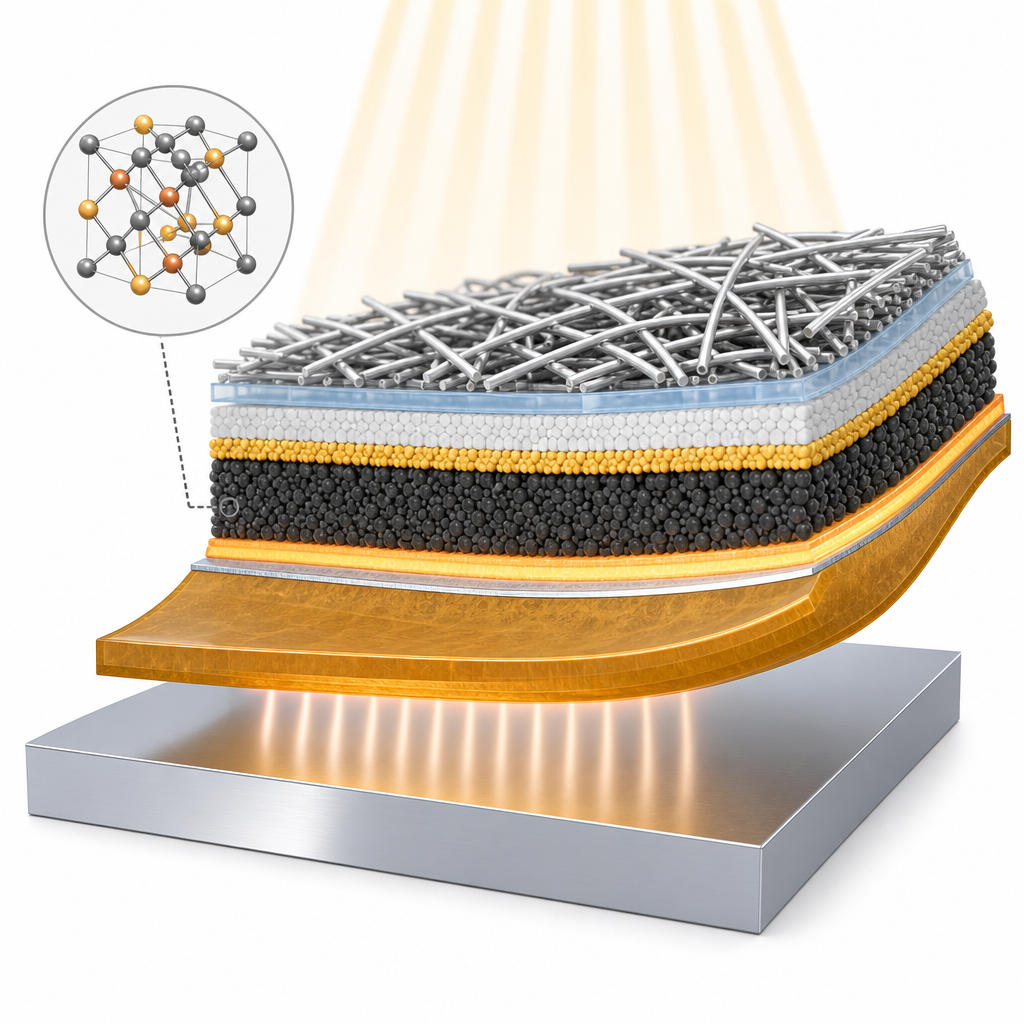
ACS Material's silver nanowire ink was central to the device architecture as the top transparent conductive electrode. The Methods section specifies: "AgNW dispersed in isopropanol at a concentration of 20 mg/mL were purchased from ACS Material." For device fabrication, the stock ink was diluted with isopropanol to 0.8 mg/mL and deposited using a Sonotek ExactaCoat ultrasonic spray system equipped with a 120 kHz nozzle, at a raster spacing of 3 mm, speed of 10 mm/s, ink injection rate of 0.1 mL/min, air pressure of 1.6 psi, and nozzle-to-substrate height of 11.5 cm. The number of coating cycles (12, 15, or 18) controlled film thickness; 18 cycles produced a 320 nm AgNW film. AgNW films were sprayed directly onto sputtered intrinsic ZnO either to replace the ITO top contact entirely or to overlay a thinned ITO layer (50–200 nm) as a hybrid electrode, providing the mechanical compliance the brittle oxide lacked while preserving optical transparency.
The PLO process used a PulseForge Invent IX2-95X tool delivering a 150 µs broadband pulse (200–1100 nm) at fluences up to 4.55 J/cm², driving the W/Ti light-absorber layer to 855 °C while the polyimide-side surface stayed below 200 °C and re-equilibrated within 50 ms. SEM and XRD confirmed that CuInSe2 nanocrystal, CdS, and ZnO layers retained their morphology and chalcopyrite crystal structure after lift-off. Devices with pure ITO top contacts cracked extensively and stopped working after PLO. Devices with AgNW-only top contacts (320 nm) survived intact, with average PCE decreasing only slightly from 1.8% to 1.6%, while open-circuit voltage and fill factor were unchanged and only the short-circuit current dropped — a decrease attributed to device aging rather than PLO, since glass-supported control devices showed the same Jsc trend. The hybrid ITO/AgNW electrode delivered the best results: with 50 nm ITO plus 18 AgNW coating cycles, 100% of devices retained near-original PCE after lift-off, versus only 5% for the 200 nm ITO baseline. Champion efficiency reached 2.8% before and 2.2% after PLO. Sheet resistance of the AgNW films was ~5 Ω/sq, lower than the ~19 Ω/sq of the sputtered ITO.
The approach is directly relevant to flexible and lightweight photovoltaics for building- and product-integrated solar, wearables, IoT power harvesting, and high-specific-power applications such as stratospheric platforms and spacecraft. Because PLO accommodates large illumination areas and microsecond pulse durations, it is well suited to roll-to-roll manufacturing of polymer-supported optoelectronic devices, including OLEDs, flexible thin-film transistors, and other devices that require a transparent conductive electrode but cannot survive the mechanical stress associated with ITO during release. The authors note that other solution-processable nanocrystal absorbers (perovskites, PbS, PbSe, CdTe) could be integrated similarly, broadening the platform.
For researchers developing flexible electrodes, ITO replacements, or photonic-lift-off-compatible device stacks, the silver nanowire dispersions available from ACS Material provided a straightforward solution-processable conductor that worked under spray-coating conditions and survived high-fluence pulsed processing. The paper demonstrates that off-the-shelf AgNW inks can be used directly as the top current collector in functioning thin-film solar cells, and that hybrid AgNW/ITO architectures offer a practical compromise between mechanical durability and carrier-collection efficiency for next-generation flexible optoelectronics.How ACS Material products were used
- Silver Nanowire (AgNW) dispersion in isopropanol, 20 mg/mL (Nanowire Series) — “AgNW dispersed in isopropanol at a concentration of 20 mg/mL were purchased from ACS Material.”
- Silver Nanowire dispersion in isopropanol (20 mg/mL) (Nanowire Series) — “AgNW dispersed in isopropanol at a concentration of 20 mg/mL were purchased from ACS Material.”
Product Performance in this StudyThe ACS Material silver nanowire dispersion was used to form the flexible top transparent conductive electrode that replaced or augmented the brittle ITO layer. AgNW films withstood photonic lift-off without cracking and, combined with thin ITO, enabled flexible CuInSe2 nanocrystal solar cells reaching a champion 2.8% PCE before and 2.2% after lift-off.
Related product categories
Frequently asked questionsWhy replace ITO with silver nanowires in flexible solar cell top contacts?
Sputtered ITO is mechanically brittle and cracks during lift-off processes that release thin polymer-supported devices from rigid carriers. Cracking destroys lateral conductivity and breaks the photovoltaic device. Silver nanowire (AgNW) networks deposited from solution form a percolating conductor that flexes with the polymer substrate. In this study, replacing ITO with 320 nm AgNW films or a thin ITO/AgNW hybrid enabled crack-free photonic lift-off and preserved near-original power conversion efficiency.
What concentration of silver nanowire dispersion is used for spray-coated transparent electrodes?
The researchers started with a 20 mg/mL silver nanowire dispersion in isopropanol purchased from ACS Material and diluted it to 0.8 mg/mL for ultrasonic spray coating. Films were deposited at 10 mm/s with 3 mm raster spacing, 0.1 mL/min injection, 1.6 psi atomization, and an 11.5 cm nozzle-substrate distance. Eighteen spray cycles produced a 320 nm AgNW film with roughly 5 Ω/sq sheet resistance, lower than the 19 Ω/sq of comparable sputtered ITO.
How does photonic lift-off compare to laser lift-off for flexible device manufacturing?
Photonic lift-off uses a broadband flash lamp (200–1100 nm) delivering microsecond pulses across a large area, while laser lift-off relies on narrow excimer beams. The flash-lamp approach avoids ashing of polymers because the metal absorber layer blocks direct UV illumination of the substrate, and it scales easily to large areas and roll-to-roll lines. Beam-width limitations and UV-induced damage that hinder laser lift-off throughput are avoided, enabling higher manufacturing speeds.