-
Silver Nanowires for WS2 Plasmonic PL - UT Austin, 2017
Jun 19, 2026 | ACS MATERIAL LLCCheng, F. et al. (2017). Enhanced Photoluminescence of Monolayer WS2 on Ag Films and Nanowire–WS2–Film Composites. *ACS Photonics*. https://doi.org/10.1021/acsphotonics.7b00152
University of Texas at Austin · ACS Photonics · 2017
UT Austin researchers used ACS Material silver nanowires (~120 nm) on monolayer WS2-Ag film hybrids, boosting photoluminescence ~38x via exciton-SPP coupling.
About this research
Researchers at the University of Texas at Austin used silver nanowires from ACS Material (nominal diameter ~120 nm) to construct a nanowire–WS2–Ag film composite that boosts the photoluminescence (PL) of monolayer tungsten disulfide by roughly 38 times relative to as-grown WS2 on sapphire. Reporting in ACS Photonics (2017), the team led by Chih-Kang Shih systematically determined the optimal dielectric spacer thickness between WS2 and Ag, then exploited propagating surface plasmon polaritons (SPPs) reflected from the ends of Ag nanowires to drive cyclic re-excitation of WS2 excitons. The work delivers a quantitative recipe for coupling two-dimensional transition metal dichalcogenides (TMDCs) to plasmonic nanostructures and identifies epitaxial silver films as the platform of choice.
Monolayer TMDCs such as WS2 and MoS2 are attractive light emitters for ultrathin optoelectronics, but their absolute photoluminescence quantum yield is modest because a sub-nanometer-thick semiconductor cannot absorb much light. Plasmonic nanostructures can amplify both absorption and the radiative recombination rate through near-field enhancement, yet placing an emitter too close to a metal opens non-radiative quenching channels. The community had largely adopted a ~5 nm dielectric spacer borrowed from earlier dye and III–V emitter work, without verifying that this value is correct for atomically thin TMDCs. Establishing the right spacer thickness, and the right metal film morphology, is critical for designing efficient on-chip plasmonic light sources, nanolasers, and biosensors based on 2D materials.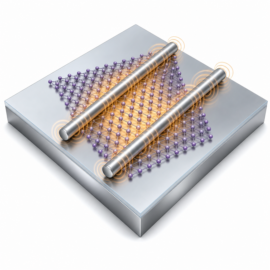
The ACS Material silver nanowires were the central plasmonic element of the composite device. After growing triangular WS2 monolayers on sapphire by chemical vapor deposition and confirming a uniform ~0.6 nm thickness by AFM, the authors transferred the flakes via a PMMA-assisted wet transfer onto either polycrystalline thermally evaporated Ag films or atomically smooth epitaxial Ag films grown by molecular beam epitaxy on Si(111). A precisely controlled Al2O3 spacer (1–5 nm) was deposited by atomic layer deposition. Silver nanowires from ACS Material with a nominal diameter of ~120 nm were then spin-cast across the sample, followed by a ~150 nm PMMA capping layer to prevent oxidation and sulfurization. As stated in the Methods: "Ag NWs (ACS Material Corp., nominal diameter ~120 nm) are spin casted across the whole sample surface." The nanowires were positioned so that part of their length lay on top of the WS2 flake and the remaining length extended onto the bare Ag film, allowing exciton-coupled SPPs to propagate along the wire, reflect from its end, and return to re-excite excitons.
The results overturn the prevailing ~5 nm spacer rule for TMDC plasmonics. The optimal Al2O3 spacer between WS2 and Ag was found to be ~1 nm, attributed to the extreme 2D geometry and ~1–1.5 nm exciton diameter of monolayer WS2. At this thickness, WS2 PL on a thermal Ag film increased by more than an order of magnitude (~13x at 79 K) compared with WS2 on sapphire, and by ~16x on an epitaxial Ag film. The epitaxial film showed roughly half the imaginary permittivity of standard Johnson–Christy values at 2 eV and an RMS roughness of 0.32 nm versus 3.4 nm for the polycrystalline film. Adding ACS Material silver nanowires on top produced an additional PL boost of ~2.4x on the epitaxial platform but only ~1.3x on the polycrystalline platform, demonstrating that reduced SPP propagation loss on atomically smooth Ag is essential for the nanowire-mediated re-excitation mechanism. The total enhancement of ~38x over as-grown WS2 on sapphire was achieved at 79 K. Power-dependent measurements showed linear PL scaling with laser power and no peak shift or broadening, confirming the absence of plasmonic heating. Finite-element simulations confirmed that thinner spacers concentrate the dipole–SPP magnetic field and that the propagating mode along the nanowire has its electric field confined within the Al2O3 spacer.
The nanowire–WS2–film composite offers a non-resonant route to strong light–matter coupling in 2D semiconductors, useful for plasmonic nanolasers, single-photon sources, biosensors, photodetectors, and on-chip optoelectronic interconnects based on TMDCs. Because the enhancement does not rely on a sharp plasmonic resonance, the architecture tolerates spectral variation across different monolayer materials (WS2, MoS2, WSe2, MoSe2) and could be extended to van der Waals heterostructures. The clear demonstration that epitaxial Ag substantially outperforms thermally evaporated Ag for nanowire-mediated re-excitation also points toward broader use of single-crystalline metal films in quantum photonics and integrated plasmonics. Future work may exploit smaller laser spot sizes, alternative nanowire geometries, and tailored end reflectors to further increase the Purcell factor.
For researchers building TMDC–plasmonic hybrids, the takeaway is practical: a high-quality silver nanowire with a well-defined diameter can serve as a deterministic SPP waveguide and reflector for monolayer emitters. The silver nanowires used here are available from ACS Material, along with related metal nanowires, CVD 2D materials, and TEM-grade graphene supports. The product mapping above links to the silver nanowire catalog page so that procurement and replication of these plasmonic light-emission experiments are straightforward.How ACS Material products were used
- Silver Nanowire (~120 nm nominal diameter) (Nanowire Series) — “Ag NWs (ACS Material Corp., nominal diameter ~120 nm) are spin casted across the whole sample surface and then a layer of PMMA (~150 nm) was spin coated on top to protect Ag NW from degradation”
Product Performance in this StudyThe silver nanowires from ACS Material were the key plasmonic component placed atop the WS2-Ag film hybrid. They guided exciton-coupled surface plasmon polaritons that reflected from the wire ends and re-excited excitons in monolayer WS2, providing an additional ~2.4x photoluminescence enhancement beyond the WS2-Ag film alone.
Related product categories
Frequently asked questionsWhy are silver nanowires used to enhance photoluminescence in monolayer WS2?
Silver nanowires support surface plasmon polaritons that couple to WS2 excitons and reflect from the wire ends, returning to re-excite excitons along their propagation path. This cyclic re-excitation enhances both exciton generation and spontaneous emission rate. In this study, ACS Material silver nanowires of ~120 nm diameter added a ~2.4x photoluminescence boost on top of the WS2-Ag film hybrid, contributing to an overall ~38x enhancement over WS2 on sapphire.
What is the optimal dielectric spacer thickness between WS2 and a silver film for plasmonic PL enhancement?
The University of Texas at Austin team found the optimal Al2O3 spacer between monolayer WS2 and a silver film to be approximately 1 nm, much thinner than the ~5 nm value previously assumed for emitter-metal systems. At 1 nm, photoluminescence increases by more than an order of magnitude. The unusually small optimum is attributed to the 2D geometry of WS2 and the small ~1-1.5 nm exciton diameter, which changes the distance dependence of plasmon-exciton coupling.
Why do epitaxial silver films outperform thermal silver films in WS2 plasmonic devices?
Epitaxial silver films have RMS roughness around 0.32 nm versus 3.4 nm for thermally evaporated polycrystalline films, and roughly half the imaginary permittivity at 2 eV. These factors reduce surface scattering and ohmic loss of surface plasmon polaritons, allowing them to propagate farther along nanowires before being absorbed. The result is a stronger nanowire-mediated re-excitation of WS2 excitons, raising the additional PL enhancement from ~1.3x on polycrystalline films to ~2.4x on epitaxial films.