-
Single Layer Graphene for Perovskite-Silicon Tandems - Zhejiang University, 2021
Jun 03, 2026 | ACS MATERIAL LLCHang, P. et al. (2021). Technoeconomically competitive four-terminal perovskite/graphene-silicon tandem solar cells with over 20% efficiency. *Journal of Energy Chemistry*. https://doi.org/10.1016/j.jechem.2021.07.031
Journal of Energy Chemistry · 2021
Zhejiang University used ACS Material single-layer graphene to build a low-temperature graphene-silicon Schottky cell, enabling a 4-T perovskite tandem over 20% efficiency.
About this research
Researchers at Zhejiang University used commercial single-layer graphene purchased from ACS Material to build a low-temperature-processed graphene/silicon (Gr/Si) Schottky-junction solar cell, then combined it with a wide-bandgap perovskite top cell to demonstrate the first four-terminal (4-T) perovskite/graphene-silicon (PGS) tandem with a power conversion efficiency of 20.37%. The graphene was transferred onto n-type silicon at room temperature and chemically doped, yielding a standalone Gr/Si cell efficiency of 13.56%. Paired with a 1.76 eV semitransparent perovskite cell (13.35%), the resulting tandem avoids the costly high-temperature steps of conventional crystalline-silicon devices while delivering a competitive levelized cost of electricity (LCOE).
Perovskite/silicon tandems are the leading route to push single-junction photovoltaics beyond the Shockley-Queisser limit, with certified efficiencies above 29%. However, the crystalline silicon bottom cells require texturization, ion diffusion, passivation and metallization, which raise cost and use environmentally harsh etching solutions at high temperature. Graphene/silicon Schottky-junction cells offer an attractive alternative because nearly the entire fabrication can be carried out at room temperature, minimizing energy loss and simplifying processing. This makes them well matched to perovskite top cells, which also favor low-temperature processing. The open challenge is interface engineering between graphene and silicon, plus the unstable quality of transferred graphene, which has limited Gr/Si efficiencies. This work tackles both cost and integration to show a technoeconomically competitive tandem.
The ACS Material single-layer graphene (SLG) was central to the bottom cell. After preparing a TiO2 colloid as an anti-reflection layer, the team used commercial SLG bought from ACS Material together with n-type <100> silicon wafers (1-10 Ω·cm). A poly(methyl methacrylate) (PMMA) transfer method moved the graphene from copper onto the silicon: PMMA was spin-coated at 6000 rpm, ammonium persulfate etched away the copper, and the PMMA/graphene film was rinsed and laid onto the wafer. The stack was heat-treated in a pipe furnace under argon at 160 °C for 4 h to vaporize PMMA and improve the graphene-silicon interface contact, with optional acetone fumigation to remove residue. Nitric acid (HNO3) doping increased carrier density and built-in potential, while a LiF/Al back contact reduced the Schottky barrier and surface recombination. A 100 nm gold front electrode completed the device. The graphene thus functions as both the transparent junction-forming layer and the carrier-collecting electrode of the Schottky cell.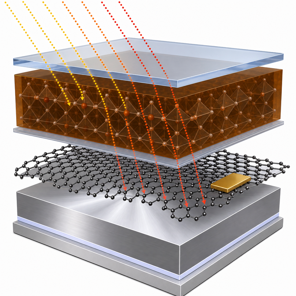
The optimized Gr/Si solar cell achieved an open-circuit voltage of 557 mV, a short-circuit current density of 33.58 mA/cm2, a fill factor of 72.53%, and a PCE of 13.56%; EQE-integrated current density of 33.55 mA/cm2 matched the J-V result. For the perovskite top cell, an Cs0.12FA0.83MA0.05Pb(I0.6Br0.4)3 absorber annealed at 150 °C gave the best film quality, longest PL lifetime and a 1.76 eV bandgap. Replacing Li-salt/TBP doping with FN-Br-doped Spiro-OMeTAD allowed an ultra-thin ~60 nm hole transport layer, raising average transmittance above 88% between 700 and 1200 nm (about 8% higher than conventional spiro). The opaque perovskite cell reached 18.57% PCE (VOC 1.21 V, JSC 19.56 mA/cm2, FF 78.46%) and retained 87% of efficiency after 100 h light soaking. The semitransparent perovskite cell delivered 13.35% (VOC 1.18 V, JSC 16.12 mA/cm2, FF 70.26%) with ~82% average transmittance. Filtered through the perovskite, the Gr/Si cell still produced 7.02%, summing to a 4-T tandem efficiency of 20.37%. A bottom-up cost model estimated module costs of 0.413 $/W (PGS) versus 0.515 $/W (PS), giving an LCOE of 5.36 US cents/kWh at 20% PCE, comparable to PS modules at 27%.
This low-temperature, low-cost approach enables perovskite/silicon tandems that sidestep the most expensive crystalline-silicon process steps, making them attractive for scalable photovoltaic manufacturing. Because Gr/Si cells can be made largely at room temperature and are amenable to roll-to-roll graphene transfer and printed device layers, the work points toward cheaper module production. The authors note that Gr/Si efficiency (13.56%) is still far from the 25.5% theoretical limit, leaving substantial headroom; improving rear-surface recombination and graphene-silicon interface quality could lift tandem performance well beyond 20%. The methodology is relevant to flexible photovoltaics, building-integrated PV, and other graphene-silicon optoelectronic devices.
For researchers pursuing graphene-silicon solar cells or 2D-material electrodes, the quality and consistency of the transferred graphene strongly influence device yield. The single-layer graphene used here is available from ACS Material's graphene catalog, alongside related CVD graphene on copper and transfer products, supporting groups working on tandem photovoltaics, transparent conductors and Schottky-junction devices. The paper's quantitative cost and efficiency analysis provides a useful benchmark for evaluating graphene as a practical, low-temperature alternative to conventional silicon cell front structures.How ACS Material products were used
- Single Layer Graphene (SLG) (Graphene Series) — “Commercial single-layer Graphene (SLG, bought from ACS Material) and n-type <100> Si wafers (1 ~ 10 X.cm, Resemi Co., Ltd.) were used to fabricate the solar cells.”
Product Performance in this StudyACS Material single-layer graphene served as the Schottky-junction electrode/active layer of the bottom Gr/Si cell, enabling a low-temperature-processed device with 13.56% efficiency and a 4-T tandem above 20%.
Related product categories
Frequently asked questionsHow is single-layer graphene used in a graphene-silicon solar cell?
Single-layer graphene is transferred onto n-type silicon to form a Schottky junction, serving as both the junction-forming transparent layer and the carrier-collecting electrode. In this study the graphene was moved from copper using a PMMA method, annealed in argon at 160 °C, then doped with HNO3, yielding a room-temperature-processed cell with 13.56% efficiency.
Why are graphene-silicon Schottky cells attractive for perovskite tandems?
Graphene/silicon Schottky cells can be fabricated almost entirely at room temperature, avoiding the costly texturization, ion diffusion, passivation and metallization steps of conventional crystalline silicon. This low-temperature, low-cost processing matches perovskite top cells, enabling four-terminal tandems with competitive levelized cost of electricity, here 5.36 US cents/kWh at 20% efficiency.
What efficiency did the four-terminal perovskite/graphene-silicon tandem achieve?
The four-terminal tandem reached 20.37% power conversion efficiency, combining a semitransparent 1.76 eV perovskite top cell at 13.35% with a graphene/silicon bottom cell that produced 7.02% when filtered. The standalone graphene/silicon cell delivered 13.56%, marking the first reported perovskite-based graphene/silicon tandem above 20%.