-
Single-Layer Graphene in 2D Perovskite Solar Cells - LBNL, 2020
May 28, 2026 | ACS MATERIAL LLCFuente, M. S. d. l. et al. (2020). Enhanced charge carrier transport in 2D perovskites by incorporating single-walled carbon nanotubes or graphene. *ACS Energy Letters*. https://doi.org/10.1021/acsenergylett.9b01821
Lawrence Berkeley National Laboratory · ACS Energy Letters · 2020
LBNL researchers used ACS Material single-layer graphene to enhance charge transport in 2D perovskite solar cells, doubling power conversion efficiency.
About this research
Researchers at Lawrence Berkeley National Laboratory used single-layer graphene supplied by ACS Material to nearly double the power conversion efficiency of two-dimensional (2D) Ruddlesden–Popper perovskite solar cells, raising pristine BA2MA3Pb4I13 devices from 4.56% to 6.17% efficiency with graphene and to 9.03% with co-incorporated semiconductor single-walled carbon nanotubes. Published in ACS Energy Letters (2020), the paper demonstrates a simple solution-blending strategy that bypasses the demanding crystal-orientation control normally required to make 2D perovskites competitive photovoltaics. By embedding conductive carbon nanostructures inside less-ordered films, the team created direct charge-transport pathways across the insulating organic spacers that otherwise throttle carrier extraction in layered perovskites.
Two-dimensional hybrid perovskites have attracted intense interest as moisture- and UV-stable alternatives to 3D methylammonium lead iodide, but their long organic spacer cations act as potential barriers that hinder photogenerated carrier transport. The state-of-the-art response has been to engineer highly crystalline films with vertical alignment of the inorganic slabs through hot-casting, additive engineering, or second-spacer chemistry. These methods raise efficiency in small samples but are difficult to scale. The Berkeley team asked whether the transport problem could instead be solved by inserting one-dimensional or two-dimensional carbon conductors directly into the film, providing percolation paths between inorganic domains and from those domains to the electrodes. This question matters for hybrid photovoltaics, low-light indoor solar harvesting, and any optoelectronic device using Ruddlesden–Popper perovskite absorbers.
The ACS Material single-layer graphene was specified at 0.6–1.2 nm thickness with flake diameters of 0.4–5 µm. The team dispersed it in dimethylacetamide at 10 mM by sonication for one hour and stirred the blend overnight before mixing with the BA2MA3Pb4I13 perovskite precursor. Films were spin-coated at 2000 rpm for 15 s and annealed at 120 °C for 10 minutes following Chen's reported procedure. Inverted planar solar cells were built in an ITO/PEDOT:PSS/perovskite/PCBM/C60/Al architecture, allowing direct benchmarking against pristine 2D perovskite and a 3D CH3NH3PbI3 control. To isolate transport effects from morphology effects, alumina nanoparticles at the same molar loading were used as an inert control, confirming that the lifetime improvements were not due to incidental film rearrangement.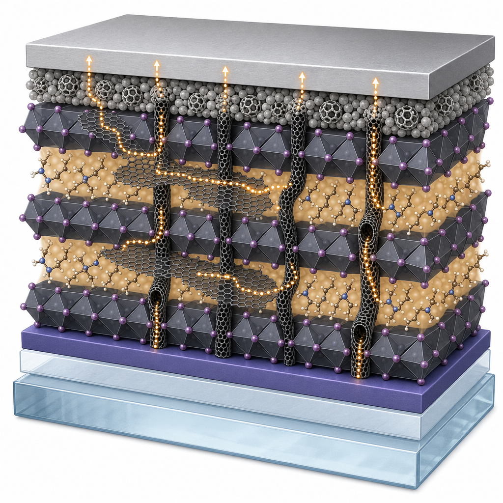
Transient photoluminescence decay confirmed substantially longer carrier lifetimes for both the graphene- and SWCNT-loaded 2D perovskite, while steady-state PL showed small redshifts (1.63 eV for the graphene composite vs. 1.65 eV pristine) consistent with mild lattice perturbation. Diffraction-limited PL mapping (~500 nm) revealed no micrometer-scale phase separation, ruling out the formation of isolated graphene-rich 3D-like islands. GIWAXS analysis showed that adding SWCNTs increased the through-plane crystallite grain size of the <111> reflection, important for vertical charge transport, while graphene slightly improved orientational order of the <002>/<200> reflection without enlarging grains. At the device level, J–V curves at 10 mV/s yielded Jsc = 10.7 mA/cm² and PCE = 6.17% for graphene-loaded cells versus 8.6 mA/cm² and 4.56% for pristine 2D, with SWCNT-loaded cells reaching 14.4 mA/cm² and 9.03%. Voc remained near 0.95–0.99 V across all samples, ruling out short circuits between HTL and ETL. External quantum efficiency, light-intensity-dependent Jsc, and UPS measurements together attributed the photocurrent gain to faster carrier extraction rather than enhanced photogeneration. Statistics across 40 cells per condition confirmed the trend.
The approach is directly relevant to scalable manufacture of stable hybrid perovskite photovoltaics, where 2D Ruddlesden–Popper compositions are favored for humidity and UV resistance but penalized by transport losses. Beyond solar cells, the same nanocarbon-percolation concept could benefit 2D-perovskite light-emitting diodes, photodetectors, and X-ray scintillators where carrier extraction limits performance. The authors note that future optimization should jointly tune additive concentration, dispersion quality, and the resulting effects on grain size and crystallite orientation. Pairing this strategy with hot-casting or second-spacer crystallization could compound efficiency gains while preserving the moisture stability advantage of layered perovskites.
For researchers working on perovskite optoelectronics, the study illustrates how a commercial 2D carbon additive—single-layer graphene from ACS Material—can deliver measurable device-level gains without bespoke synthesis. The graphene used here is available from ACS Material's Graphene Series catalog in comparable thickness and flake-size grades, supporting reproducibility and benchmarking. Maintaining consistent flake dimensions and dispersion protocols is critical, as the paper's controls confirm that improvements stem from transport bridging rather than morphological side effects.How ACS Material products were used
- Single Layer Graphene (Graphene Series) — “single-layer graphene (thickness of 0.6–1.2 nm, flake diameter of 0.4–5 µm, ACS Material) were dispersed in dimethylacetamide (10 mM) and sonicated for 1 h.”
Product Performance in this StudyThe ACS Material single-layer graphene was blended into 2D perovskite films to bridge inorganic domains, extending charge-carrier lifetimes and roughly doubling solar cell power conversion efficiency from 4.56% (pristine 2D) to 6.17% (with graphene).
Related product categories
Frequently asked questionsHow does single-layer graphene improve charge transport in 2D perovskite solar cells?
Single-layer graphene flakes embedded in BA2MA3Pb4I13 films bridge inorganic perovskite domains separated by long insulating organic spacer cations. This creates direct percolation paths for electrons and holes to reach the transport layers before recombining. In the Berkeley study, graphene addition extended charge-carrier lifetimes and lowered series resistance near open-circuit voltage, nearly doubling power conversion efficiency from 4.56% to 6.17% without altering the optical bandgap or charge generation.
Why are 2D perovskites preferred over 3D perovskites for solar cells?
Two-dimensional Ruddlesden–Popper perovskites use long organic spacer cations that act as hydrophobic barriers against moisture, sharply reducing humidity-driven degradation. They also suppress ion migration under illumination, which improves operational stability under UV light, oxygen, and heat compared with 3D methylammonium lead iodide. The trade-off is reduced power conversion efficiency due to higher exciton binding energy and slower carrier transport across the organic layers, which the present study addresses with carbon nanostructure additives.
What graphene specifications are suitable for perovskite photovoltaic blending?
The Berkeley team used single-layer graphene with 0.6–1.2 nm thickness and 0.4–5 µm flake diameters, dispersed in dimethylacetamide at 10 mM with one hour of sonication. Thin flakes ensure compatibility with ~200 nm thick perovskite films without disrupting crystallization, while micrometer-scale lateral dimensions provide enough bridging length between inorganic domains. Stable dispersions are essential; the prepared blends remained colloidally stable for several days before spin-coating.