-
TERS of Nano-Patterned Graphene & GO - PNNL, 2018
Jun 12, 2026 | ACS MATERIAL LLCBhattarai, A. et al. (2018). Tip-enhanced Raman scattering from nanopatterned graphene and graphene oxide. *Nano Letters*. https://doi.org/10.1021/acs.nanolett.8b01690
Pacific Northwest National Laboratory · Nano Letters · 2018
PNNL researchers use pulsed-force nano-indentation to unlock tip-enhanced Raman from ACS Material graphene oxide and Trivial Transfer Graphene on gold.
About this research
Researchers at Pacific Northwest National Laboratory, working with ACS Material single-layer graphene oxide dispersion and Trivial Transfer® Graphene, demonstrated that pulsed-force nano-indentation can locally switch on tip-enhanced Raman scattering (TERS) signals from otherwise pristine 2D carbon flakes deposited on gold. Using a sharp single-crystal diamond AFM probe to inscribe nanoscale indentation patterns, the team converted in-plane Raman modes into TERS-active features by generating out-of-plane structural protrusions, and then mapped the resulting D- and G-band intensities with ~15 nm spatial resolution. The result extends TERS to material systems normally invisible to gap-mode nanoscopy.
Tip-enhanced Raman spectroscopy is one of the most powerful tools for nanoscale chemical imaging, capable of single-molecule sensitivity and nanometer precision. However, in the gap-mode geometry between a metallic tip and a metallic substrate, the enhanced optical field is oriented along the tip axis, perpendicular to the sample plane. This means flat 2D materials such as pristine graphene and graphene oxide, whose vibrational modes lie predominantly in-plane, give very faint TERS signals. Only edges, wrinkles, strain sites, and defects typically light up. This is a serious limitation for researchers trying to use TERS to identify or characterize uniform regions of graphene and related 2D materials, where the most interesting electronic behavior occurs in the flat, undisturbed regions of the lattice.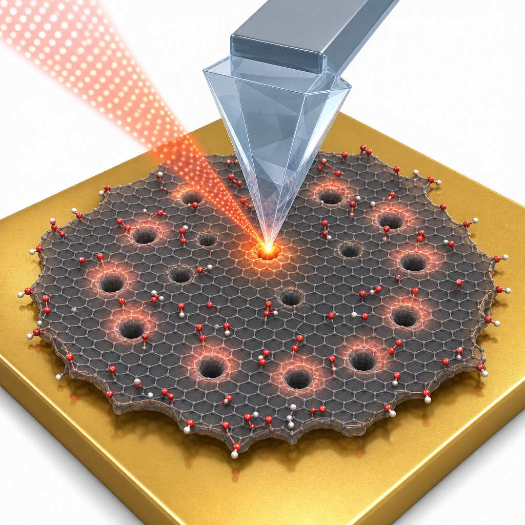
The ACS Material graphene oxide was supplied as an ethanol suspension and drop-cast onto gold-coated glass slides modified with a 4th-generation amino-terminated PAMAM dendrimer, forming a polymer/gold bilayer that supported individual graphene oxide flakes. For the pristine graphene experiments, Trivial Transfer® Graphene from ACS Material was transferred directly onto a non-modified gold-coated substrate, and the PMMA support film was removed by repeated acetone rinses. A D300-series single-crystal diamond probe (k ≈ 40 N/m, f ≈ 300 kHz) with a tip radius near 5 nm was then used to inscribe nano-indentation patterns via pulsed-force lithography. A separate gold-coated silicon TERS probe (k ≈ 7 N/m, f ≈ 150 kHz) collected the TERS maps under 638 nm laser excitation, incident at 65° to the surface normal through a 100× air objective, using a SpecTop™ semi-contact mapping mode on an Omegascope-R platform coupled to a Horiba XploRA spectrometer.
Correlated AFM and TERS images over 1.5 × 0.85 µm² regions of the graphene oxide flakes showed that natural folds and creases produced strong D-band (~1350 cm⁻¹) and G-band (~1600 cm⁻¹) signals, while pristine flat regions remained essentially TERS-silent. When the team inscribed the word "TERS" over a 1.0 × 0.5 µm² area of graphene oxide using pulsed-force lithography, AFM cross-sections revealed resolution-limited nano-holes flanked by buckled out-of-plane protrusions. The hyperspectral TERS maps reproduced the inscribed pattern with both D- and G-band contrast localized to a single 15.6 nm pixel, demonstrating that the introduced defects are highly confined. The TERS count rates from nano-indented sites were comparable to those from natural wrinkles, confirming that controlled indentation reproduces the same activation mechanism as intrinsic corrugations. In a second experiment, circular patterns inscribed across a graphene/gold boundary using the Trivial Transfer Graphene sample showed D-band TERS contrast only on the graphene-covered regions; residual PMMA islands and bare gold showed no Raman activation, confirming that the nano-indentations act on the 2D layer itself rather than the underlying substrate.
The ability to selectively turn on TERS signals in user-defined nanoscale regions of 2D materials opens new opportunities for chemical fingerprinting, defect engineering, and band-structure modification on graphene, graphene oxide, and related layered systems. The same scanning probe platform can draw nano-lithographic patterns, perform high-resolution AFM, and acquire hyperspectral TERS maps, making it attractive for nanoelectronics prototyping, quantum-material studies, sensor fabrication, and on-demand defect creation for spintronics or catalysis research. The authors note that further work with lithographically tailored tips could give finer control over defect geometry, and that tailored optical fields may eventually allow TERS of truly pristine graphene without invasive perturbation.
For researchers working on 2D materials, the study provides a practical recipe combining a well-defined graphene oxide source, a clean monolayer-graphene transfer product, and a scanning-probe nano-indentation protocol. Both the single-layer graphene oxide ethanol dispersion and the Trivial Transfer® Graphene used here are available from ACS Material, along with related CVD graphene, h-BN, and other 2D-material products supporting TERS, AFM, and Raman characterization workflows.How ACS Material products were used
- Single Layer Graphene Oxide Dispersion (ethanol suspension) (Graphene Series) — “Single-layer graphene oxide (ethanol suspension, ACS Materials) was deposited on gold coated glass slides”
- Trivial Transfer® Graphene (Trivial Transfer Series) — “Trivial Transfer Graphene (ACS Materials) was deposited on similar non-modified gold-coated substrate and rinsed several times with acetone”
Product Performance in this StudyThe ACS Material single-layer graphene oxide dispersion provided well-defined flakes that, after pulsed-force nano-indentation, produced clearly resolved D- and G-band TERS signals localized to single 15.6 nm pixels, validating the nano-indentation enhancement protocol.
Related product categories
Frequently asked questionsWhy are pristine graphene and graphene oxide difficult to detect by tip-enhanced Raman spectroscopy?
In the gap-mode TERS geometry, the enhanced optical field at the tip-sample junction is oriented along the tip axis, perpendicular to the sample plane. Pristine graphene and graphene oxide are flat sheets whose Raman-active vibrations are predominantly in-plane, so their polarizability derivative tensors have weak projections along the surface normal. This selection rule makes uniform regions nearly TERS-silent; only edges, wrinkles, strain, and defects light up.
How does pulsed-force nano-indentation enhance TERS signals from 2D materials?
A sharp single-crystal diamond AFM probe is driven into the 2D flake at user-defined points to create resolution-limited nano-holes flanked by out-of-plane protrusions. These local out-of-plane distortions tilt vibrational modes so that their polarizability derivatives gain a component along the tip axis, coupling them to the gap-mode field. The result is bright, spatially localized D- and G-band TERS signals confined to single sub-20 nm pixels.
What sample preparation was used for the ACS Material graphene oxide and Trivial Transfer Graphene in this study?
Single-layer graphene oxide from ACS Material, supplied as an ethanol suspension, was drop-cast onto 50 nm gold-coated glass slides modified with a fourth-generation amino-terminated PAMAM dendrimer. Trivial Transfer Graphene was transferred onto non-modified gold-coated substrates and rinsed multiple times with acetone to remove the PMMA support film, giving clean monolayer graphene on gold suitable for AFM nano-indentation and TERS imaging.