-
Graphene Nanoplatelet Photocathodes on GaAs - TU Darmstadt, 2014
May 26, 2026 | ACS MATERIAL LLCYilmazoglu, O. et al. (2014). Photocathodes based on graphene nanoplatelet emitters on semi-Insulating GaAs photoswitch. *2014 27th International Vacuum Nanoelectronics Conference (IVNC)*. https://doi.org/10.1109/ivnc.2014.6894740
2014 27th International Vacuum Nanoelectronics Conference (IVNC) · 2014
TU Darmstadt and Shizuoka University built a graphene nanoplatelet photocathode on semi-insulating GaAs with 1.5 V/µm turn-on field and >200 on/off ratio.
About this research
Researchers at Technische Universität Darmstadt, working with collaborators at Shizuoka University, demonstrated a photo-modulated cold-cathode electron source by combining plasma-exfoliated graphene nanoplatelets purchased from ACS Material with a semi-insulating gallium arsenide (GaAs) photoswitch. The hybrid device achieved a low turn-on field of about 1.5 V/µm and a field-emission on/off ratio greater than 200 under laser triggering. The work, published in the 2014 27th International Vacuum Nanoelectronics Conference proceedings, shows a route to compact optically-gated electron sources for X-ray imaging and miniaturized high-frequency vacuum tubes.
Compact, optically-triggered electron sources are critical for next-generation X-ray imaging, biomedical diagnostics, and high-frequency vacuum electronics that need to operate beyond the cutoff frequencies of solid-state GaAs and InP devices. Traditional thermionic cathodes are bulky, slow to modulate, and incompatible with on-wafer integration. Cold field emitters offer fast response and integration potential, but until now most candidate materials either required CVD growth at temperatures incompatible with GaAs substrates or suffered from high turn-on fields. The challenge addressed in this paper is how to integrate a robust field emitter with an ultrafast photoswitch at low process temperatures, so the resulting cathode can be triggered with simple low-power laser illumination while still delivering bunched electron emission suitable for X-ray free-electron lasers and miniaturized vacuum tubes.
The graphene nanoplatelets (GNPs) were obtained from ACS Material and prepared by plasma exfoliation with greater than 99.5% purity. The platelets have thicknesses of 2-10 nm, lateral widths of 5-10 µm, and an unusually high width-to-thickness aspect ratio of 1000-2000, which is what enables strong local field enhancement at platelet edges and the resulting low turn-on field. Because graphene CVD growth requires temperatures above 800 °C that would degrade GaAs, the authors instead developed a low-temperature gluing technique to transfer randomly oriented GNP arrays onto semi-insulating GaAs wafers at less than 100 °C. The GNP layer sits on the back side of the s.i. GaAs photoswitch (resistivity > 1×10⁷ Ω·cm, breakdown field > 2×10⁴ V/cm), with a quartz glass / ITO anode forming the diode configuration. An external 800 nm laser illuminates the GaAs through the substrate to gate the emission, and the laser position and power are not critical for modulation.
The device showed a turn-on field of about 1.5 V/µm defined at 1 µA/cm², which is competitive with much more elaborately patterned CNT or Spindt-type emitter arrays. With a 660 nm laser and 550 V bias, the photoswitch effectively held the cathode-anode voltage at 0 V in the dark and switched it to ≈100 V on illumination, producing emission currents that modulated between off and on with an on/off ratio greater than 200. Photo-modulated field emission was demonstrated at frequencies up to 300 kHz, limited by the oscilloscope measurement set-up rather than by intrinsic device physics. The GaAs photoswitch itself supports linear-mode sub-nanosecond switching at low bias and a non-linear lock-on mode at fields above 5 kV/cm where carrier avalanche provides current gain; the same switch architecture has elsewhere handled 3.7 kA and 28 kV. These numbers indicate substantial headroom for scaling the integrated photocathode to higher peak currents and faster pulse widths.
The demonstrated photocathode is targeted at optically-driven X-ray sources with high on/off ratio for X-ray imaging, miniaturized vacuum tubes operating at frequencies beyond solid-state limits, and high-charge short-pulse electron sources for X-ray free-electron lasers. The authors specifically note that replacing the s.i. GaAs photoswitch with semi-insulating InP (~50 ps carrier lifetime) or low-temperature-grown GaAs (<1 ps) would push the device into the picosecond regime suitable for FEL injectors. On-wafer integration of the laser or LED next to the GaAs photoswitch is identified as a promising follow-up that would yield a fully integrated, externally-electrical photocathode chip.
For researchers developing field emitters, photoinjectors, or vacuum micro-electronic devices, this paper is a useful reference for what plasma-exfoliated graphene nanoplatelets can deliver as a low-cost, low-temperature-compatible cold emitter material. The Graphene Nanoplatelets (2-10 nm) used here, along with related thickness grades, are available from ACS Material to groups working on similar X-ray source, FEL injector, and high-frequency vacuum device concepts.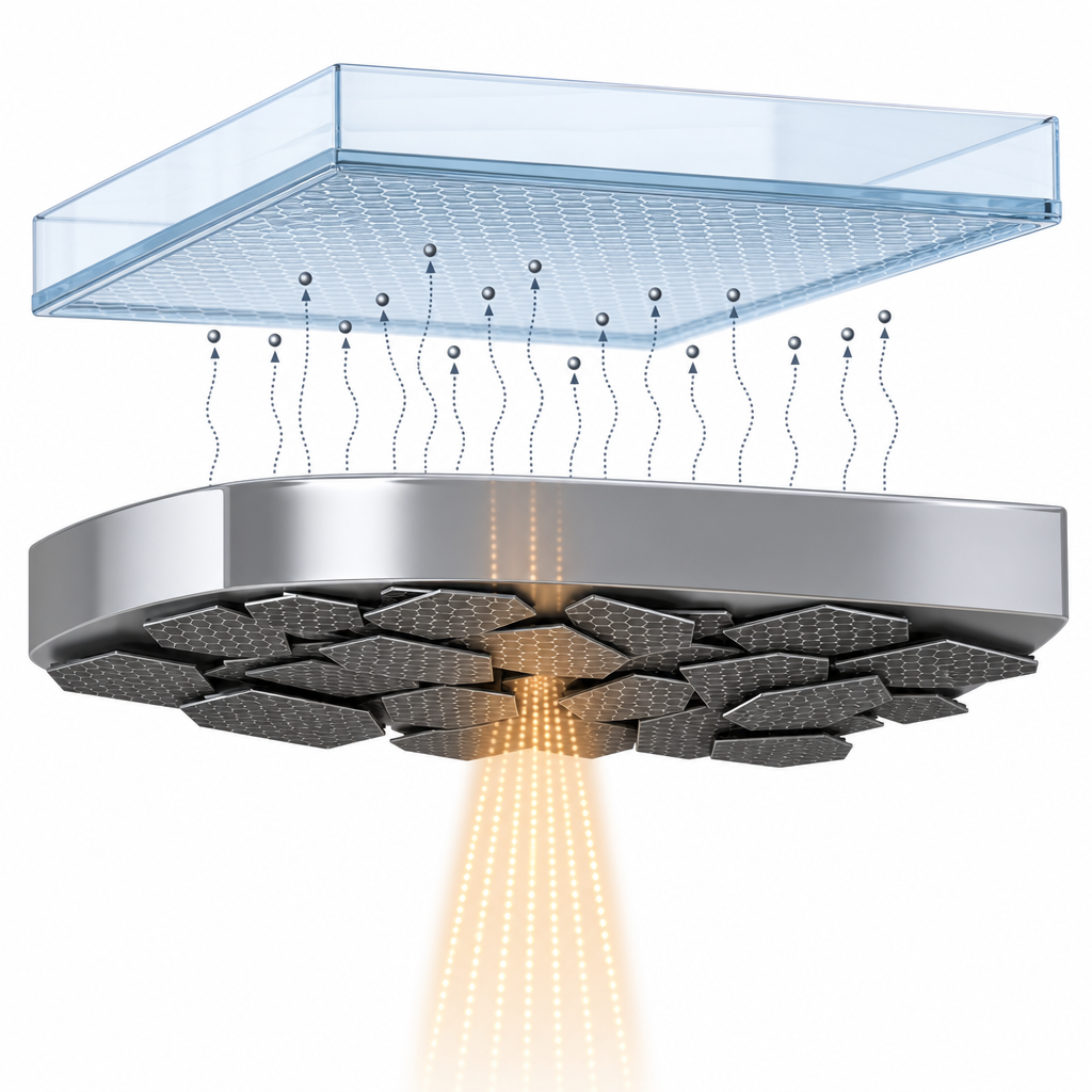
How ACS Material products were used
- Graphene Nanoplatelets (2-10nm) (Graphene Series) — “The used graphene nanoplatelets (GNPs) consist of stacks of multi-layer graphene sheets in a platelet morphology. They were purchased from ACS Materials and were prepared by plasma exfoliation with >99.5% purity. The GNPs have thicknesses in the range of 2-10 nm, width of 5-10 µm and a high graphene aspect ratio (width-to-thickness) of 1000-2000.”
Product Performance in this Study
The ACS Material graphene nanoplatelets functioned as the cold field-emission cathode, delivering a low turn-on field of approximately 1.5 V/µm at 1 µA/cm² and supporting photo-modulated emission with an on/off ratio greater than 200.
Related product categories
Frequently asked questions
Why are graphene nanoplatelets good field-emission cathodes?
Graphene nanoplatelets combine sharp atomically-thin edges with a very high width-to-thickness aspect ratio, typically 1000 to 2000 for the 2-10 nm thick platelets used in this study. That geometry concentrates the applied electric field at the platelet edges, so electrons tunnel into vacuum at a much lower macroscopic field than for bulk emitters. The team measured a turn-on field of about 1.5 V/µm at 1 µA/cm².
How does a GaAs photoswitch modulate a graphene field emitter?
The semi-insulating GaAs sits in series with the graphene cathode. In the dark it is highly resistive, so the cathode-anode voltage stays near zero and no emission occurs. When 800 nm laser light hits the GaAs, photogenerated carriers collapse its resistance, transferring the bias voltage onto the field emitter and switching emission on. This produced an on/off ratio above 200 and modulation up to 300 kHz.
What applications need optically gated photocathodes like this one?
Photo-triggered cold cathodes are attractive for compact X-ray sources used in medical and security imaging, where high on/off contrast and fast gating reduce dose and improve resolution. They are also relevant to miniaturized vacuum tubes operating above the cutoff frequencies of solid-state GaAs or InP devices, and to short-pulse high-charge injectors for X-ray free-electron lasers when paired with picosecond-lifetime photoconductors.