Across the publication set reviewed for this article, researchers at Friedrich-Alexander-Universität Erlangen-Nürnberg used transferable CVD graphene in studies spanning bilayer-dislocation mechanics, atomic-resolution imaging of covalent functionalization, liquid-phase TEM, SEM-based diffraction, and optical layer metrology. Three papers explicitly name ACS Material or Trivial Transfer® Graphene in their Methods or Experimental Sections; the remaining product-format associations come from ACS Material’s publication-matching records and are labeled accordingly. This spotlight examines what the graphene enabled — and, just as importantly, which parts of each experiment remained the researchers’ own preparation, instrumentation, and scientific work.
At a glance
Evidence map
Two kinds of evidence support this article, and this table keeps them separate. Three studies explicitly name the product in their Methods or Experimental Sections; the remaining studies are associated with specific formats through ACS Material’s publication-matching records.
| Year | Study focus | Graphene format in the record | Evidence basis |
|---|---|---|---|
| 2018 | Bilayer dislocation mechanics and switching | Nominally bilayer TTG | Named in the paper’s Methods |
| 2019 | Optical layer counting by reflectance | Single-, bi-, and multilayer CVD films | ACS publication-matching record |
| 2020 | LEND diffraction in a configured SEM | TTG (per record) | ACS publication-matching record |
| 2020 | Stacked van der Waals layer metrology | Mono-, bi-, and multilayer films | ACS publication-matching record |
| 2022 | Atomic-resolution covalent-functionalization imaging | PMMA-coated monolayer TTG | Named in the paper’s Methods |
| 2022 | Liquid-phase TEM radiolysis modeling | 6–8-layer Trivial Transfer® Graphene | Named in the paper’s Experimental Section |
| 2024 | Aperture-based dark-field STEM in SEM | Bilayer graphene (per record) | ACS matching record; public product naming not yet verified |
Related FAU study outside the selected seven: a 2019 graphene-sealed liquid-cell TEM study of gold-nanoparticle etching and growth used a different ACS Material graphene line (graphene on Quantifoil, 6–8 layers) and is covered in a separate ACS Material case study.
Who is the Spiecker group?
Prof. Erdmann Spiecker heads FAU’s Institute of Micro- and Nanostructure Research and the Center for Nanoanalysis and Electron Microscopy (CENEM), an interdisciplinary center combining electron microscopy with complementary nanoanalysis methods. The group's public profile centers on advanced and in situ electron microscopy — watching materials deform, transform, and react inside the microscope rather than only imaging the end state. Around that core sits a wider Erlangen ecosystem: co-authors from the FAU Electron Devices chair (including Dr. Andreas Hutzler) and the Fraunhofer Institute for Integrated Systems and Device Technology (IISB) appear repeatedly in the same publication cluster.
For work like this, the specimen support is not an accessory — it is part of the experiment. A freestanding, electron-transparent, atomically defined membrane lets the microscope see the physics of the film itself, and a PMMA-supported film supplied for transfer shortens the path from material preparation to the laboratory’s own downstream workflow. That is the role the records suggest ACS Material graphene played here, and the papers below show what it was used for.
Moving dislocations inside freestanding bilayer graphene
The anchor of the cluster is a 2018 Science Advances paper by Schweizer, Dolle, and Spiecker on dislocations — the line defects that govern how crystals deform — in freestanding bilayer graphene.1 The team not only imaged individual dislocations in the suspended bilayer but manipulated them mechanically at the nanoscale, in situ, reporting direct observations of properties such as dislocation line tension, dislocation–dislocation interaction, and node formation. They further described a reaction between mobile in-plane dislocations and sessile out-of-plane dislocations that changes how regions of identical stacking order (AB or AC) interconnect, and on that basis proposed the layout of a reversible "topological switch".1
The starting material is stated plainly in the paper's methods: CVD-grown, nominally bilayer graphene "(Trivial Transfer Graphene) was purchased from ACS Material", delivered on its substrate with the PMMA transfer layer in place.1 From there, everything that made the experiment remarkable — the suspension, the cleaning, the imaging strategy, the manipulation — was the group's own craft. That division of labor is worth underlining: the product's job was to be a reliable, transferable bilayer; the science was theirs.
Atomic-resolution imaging of covalent chemistry
In 2022, Dolle, Schweizer, and colleagues — together with the synthetic-chemistry group of Prof. Andreas Hirsch and theory collaborators — reported atomically resolved TEM imaging of covalently functionalised graphene in npj 2D Materials and Applications.2 The paper’s Methods state explicitly that the freestanding monolayer specimens were prepared from PMMA-coated Trivial Transfer Graphene supplied by ACS Material — released on water, transferred onto cleaned Quantifoil grids, and freed of the PMMA layer in acetone before functionalization.2 Covalent functionalization is commonly characterized through ensemble spectroscopy; directly imaging individual functional groups at atomic resolution adds a complementary structural view. The functionalization chemistry, cleaning procedure, and specimen preparation were defined entirely by the authors’ protocol.
Liquid-phase TEM and radiolysis models
The same year, an FAU-led team including Fritsch, Hutzler, and Spiecker published a liquid-phase TEM study in Advanced Science that tackled a core problem of the technique: the electron beam radiolyzes the liquid, and the resulting chemistry can drive the very nanostructure evolution being imaged.3 Using gold nanostructures as the test system, the work verified a radiolysis model by bridging scales between in situ liquid-phase TEM and X-ray methods — an important step toward making beam-driven chemistry quantitative rather than an uncontrolled artifact. The paper’s Experimental Section states that liquid encapsulation was performed using 6–8-layer Trivial Transfer® Graphene from ACS Material, transferred onto holey carbon-coated gold TEM grids.3 The multilayer format is consistent with the mechanical demands of a liquid-cell membrane, although the study did not present layer count as a controlled comparison.
A related 2019 study from the same Erlangen ecosystem — graphene-sealed microwell liquid cells for imaging gold-nanoparticle etching and growth — used a different ACS Material graphene line (graphene on Quantifoil, 6–8 layers) and is covered in a separate ACS Material case study.
New instruments and layer metrology
A recurring signature of the Erlangen cluster is that graphene is not only the specimen — it is the test object for new measurement techniques. In 2020, Schweizer, Denninger, Dolle, and Spiecker introduced low-energy nano diffraction (LEND), a versatile diffraction technique implemented in a scanning electron microscope,4 bringing crystallographic information into a specially configured SEM with a dedicated transmission and detection setup. In 2024, Denninger, Schweizer, and Spiecker extended the platform with aperture-based dark-field STEM in the SEM, using a LEND setup to select individual reflections for imaging and demonstrating diffraction-contrast analysis of extended defects in 2D materials — including Burgers-vector analysis of basal-plane dislocations in bilayer graphene, benchmarked against conventional TEM and 4D-STEM.5 Six years after the Science Advances paper, the same defects in the same material class were being read out with an SEM-based diffraction setup of their own design.
On the metrology side, Hutzler, Spiecker, and co-workers showed in 2019 that layer numbers of two-dimensional materials can be counted over large areas by tracking the wavelength shift of features in visible-reflectance spectra,6 with our records listing single-, bi-, and multilayer CVD graphene films for that study. A 2020 follow-up in Scientific Reports generalized the approach: a hybrid evaluation of reflectance change and wavelength shift, supported by a transfer-matrix optical model, that can determine the composition of stacked van der Waals heterostructures and discriminate even structurally similar materials such as graphene and hexagonal boron nitride.7 Together, these studies illustrate independent optical routes for evaluating layer count and heterostructure composition over large areas.
Practical notes from the record
Read as a publication-linked materials-use record rather than only a reading list, the cluster is instructive in three ways. First, format breadth: across the record, our publication-matching entries list bilayer TTG, PMMA-coated monolayer TTG, 6–8-layer TTG, and companion CVD graphene films — the layer count tracked the experiment, not the other way around. Second, continuity: publications span 2018 to 2024, through student generations and even as alumni moved on to other institutes — a repetition that suggests continuity in experimental needs, although the publication record alone does not establish a standardized group-wide purchasing workflow. Third, the division of labor: in every study, the film was a starting point; suspension, cleaning, functionalization, and instrumentation were the researchers' own. A support film cannot make an experiment succeed — at best it can stop being the reason one fails.
| Format in the record | Research need |
|---|---|
| Bilayer TTG | Stacking domains and dislocation mechanics |
| Monolayer TTG (PMMA-coated) | Minimum thickness for atomic-resolution chemical imaging |
| 6–8-layer graphene | Greater membrane robustness in liquid-cell configurations (a design rationale in our reading, not an author conclusion) |
| Single-, bi-, multilayer CVD films | Optical layer-counting and heterostructure metrology |
Planning a suspended-graphene, liquid-cell, or in situ microscopy workflow? Explore transferable graphene formats, or ask about custom sizes and special samples.
Explore Trivial Transfer® GrapheneWorking on biological specimens instead? The same transfer logic underpins graphene supports for cryo-EM — our evidence-based guide to graphene grids for cryo-EM covers that line of work, from the air–water interface problem to batch grid preparation.
FAQ
Which products does the record associate with this group?
Per our publication-matching records: Trivial Transfer® Graphene in bilayer, PMMA-coated monolayer, and 6–8-layer formats, plus companion CVD graphene films (single-, bi-, and multilayer) in the two metrology studies.6,7 Exact specifications for any given study are those stated in that paper's methods.
Does buying the same film reproduce these experiments?
No — and the papers make that clear. The film is the starting material; suspension, transfer onto custom supports, cleaning, functionalization, and the imaging or diffraction methodology are laboratory-specific and are described in each publication.1–5 Treat the methods sections, not the product page, as the protocol.
Why do layer counts differ from study to study?
Because the physics differs. The dislocation work required a bilayer, whose stacking order is the object of study;1,5 liquid-phase TEM used a 6–8-layer film per the paper’s Experimental Section, where mechanical demands on the membrane are higher;3 atomic-resolution chemistry imaging started from a monolayer.2 Layer count is an experimental variable, not a quality grade.
References
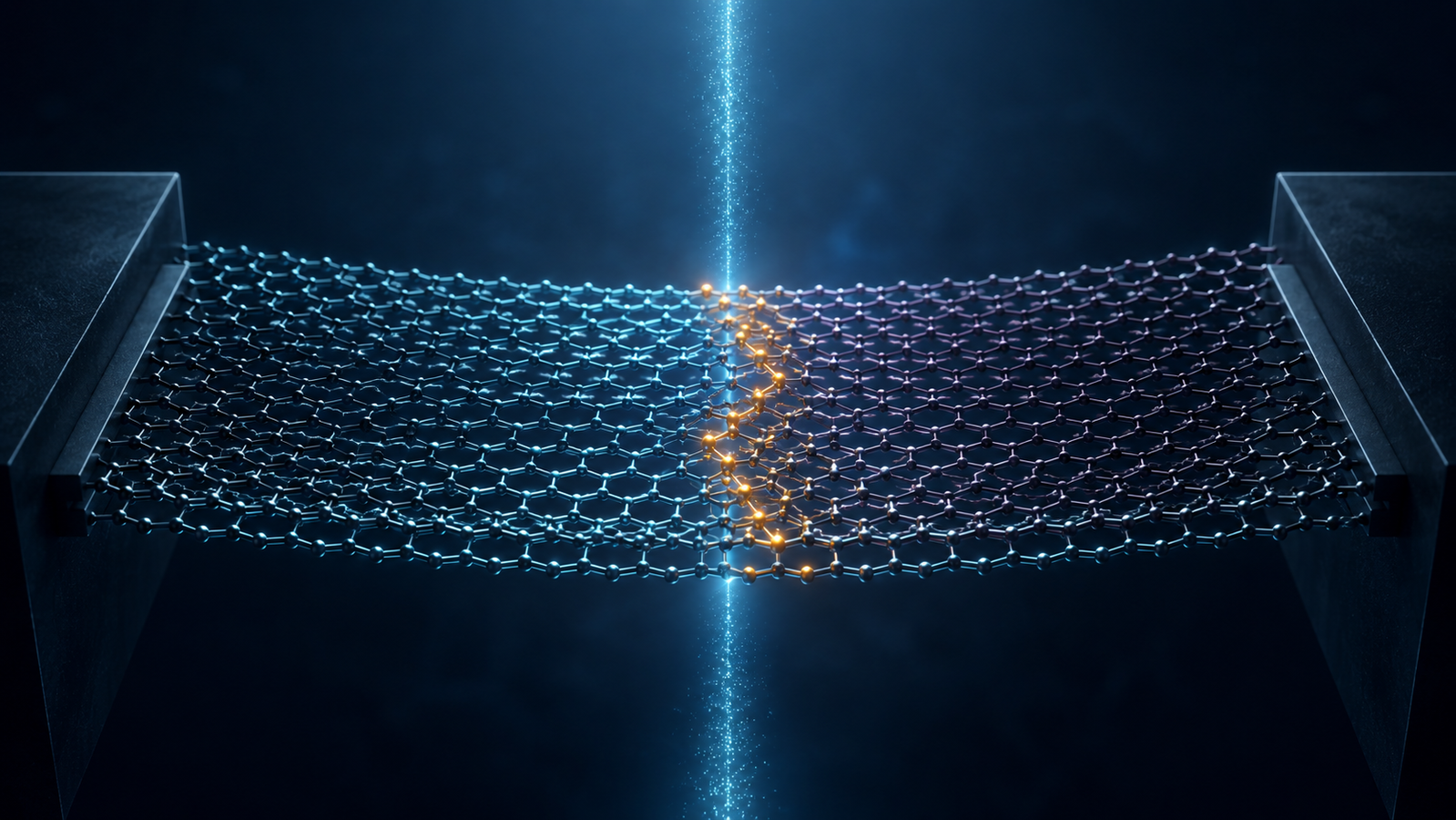
The studies described here are independent research by the named authors and institutions; ACS Material was not involved in their design, execution, or publication, and no endorsement is implied. Product associations reflect the papers' methods statements and ACS Material publication-matching records. The illustration above is an AI-generated representative rendering, not a micrograph from the cited studies. Trivial Transfer® is a trademark of ACS Material, LLC.