
Below the reach of every clamp, disc and heater line lives the measurement problem that defined nanoscale thermal science: what is the conductivity of one nanotube, one nanowire, one ribbon? The suspended micro-bridge answered it with microfabrication — two silicon-nitride membrane islands, each carrying a platinum heater-thermometer, thermally isolated on long slender beams, with the nano-object of interest laid across the gap between them1. Heat one island, read both, and the sample’s thermal conductance follows. The architecture produced landmark results — a single multiwalled carbon nanotube above 3000 W m⁻¹K⁻¹ at room temperature, two orders beyond what mat samples had suggested2 — and it also codified the two disciplines every suspended measurement since has inherited: subtract the background you measured, and budget the contacts you cannot see13.
- 1Two islands and an energy balance
- 2What it proved: the founding results
- 3The two budgets: background and contacts
- 4Interactive: watch small samples pay twice
- 5The T-type nanosensor: one suspended sensor, one attached sample
- 6Micro-bridge and the wider suspended family
- 7The method in the landscape
- 8Frequently asked questions
- 9Keep exploring the knowledge hub
- 10References
Two islands and an energy balance
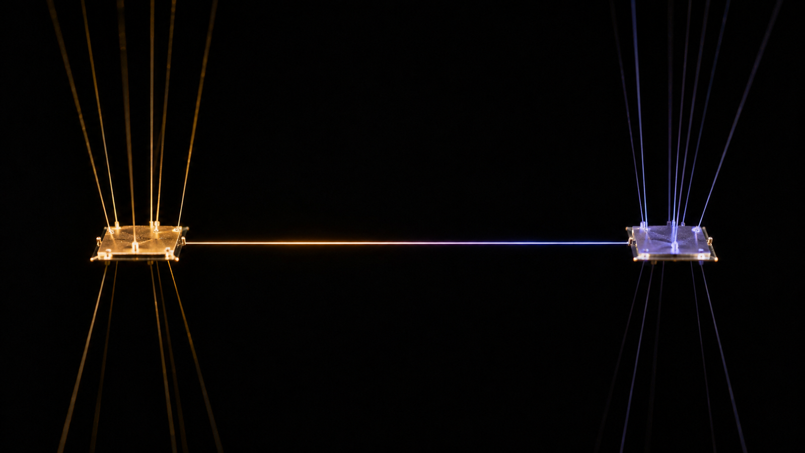
The canonical device, established by Shi and colleagues, is a batch-fabricated pair of low-stress silicon-nitride membranes, each suspended on several long, narrow beams that give the islands thermal isolation of order hundreds of nanowatts per kelvin, each carrying a serpentine platinum line that serves as both heater and resistance thermometer1. The nanostructure — nanotube, nanowire, nanobelt, later 2D flakes — is placed or grown across the gap. Pass current through one island’s heater: its temperature rises; heat crosses the sample; the sensing island warms by a smaller amount. With both temperatures read and the beams’ conductance characterized, the steady-state energy balance yields the sample’s thermal conductance directly — and, with electrodes on the same platforms, electrical conductance and Seebeck coefficient in the same sitting1.
Operation in an evacuated cryostat is not incidental: suppresses the parallel residual-gas contribution below the selected measurement resolution and gives access to the deep cryogenic-to-moderate range where phonon physics unfolds, with the exact span set by the device generation14. The vacuum requirement, the fabrication, and the sample-placement art are the method’s admission fees.
What it proved: the founding results
The single-nanotube measurement rewrote intuitions: an individual multiwalled tube conducted above 3000 W m⁻¹K⁻¹ at room temperature, with the umklapp-scattering peak near 320 K resolved — two orders of magnitude beyond mat-sample estimates, because a mat measures its junctions, not its tubes2. That lesson — ensembles measure their contact networks; single-object methods measure the object — echoes across this hub, from interface-mediated fiber assemblies to spun graphene yarns56. The platform went on to serve nanowires, ribbons and 2D flakes, and its descendants remain the reference architecture for single-nano-object thermal transport3.
The two budgets: background and contacts
Background. The islands are connected by more than the sample: the support beams conduct in parallel, and at higher temperatures radiation between the platforms joins in. The remedy is measurement, not assumption — characterize the empty-device conductance and subtract — and the arithmetic is unforgiving: the error of a subtraction grows as the sample’s share of the total shrinks, under the equal, independent-error teaching limit, the familiar √2-type amplification (unequal variances, covariance and shared calibration terms require the more general propagation model)78. A weak sample on a comparatively conductive device is a bad experiment before it begins.
Contacts. Heat enters and leaves the sample through two nanoscale junctions whose conductance is finite, variable, and in series with the quantity of interest. The community’s defenses are structural: improve the junctions with local metal deposition, vary the sample length so the contact term separates as an intercept, and bound the residual in the stated budget39. Interfacial thermal resistance is a first-class subject at this scale, not a footnote9.
Interactive: watch small samples pay twice
The simulator applies the exact background-subtraction error law and adds an illustrative contact-systematic floor. Slide the sample’s share of the measured conductance down and watch the recovered value’s error balloon — then note that the countermeasures are structural choices made before the experiment, not statistics applied after it.
The T-type nanosensor: one suspended sensor, one attached sample
The bridge’s sibling architecture inverts the topology. In the T-type nanosensor, a single suspended metallic nanofilm strip — itself both heater and resistance thermometer — spans two heat sinks, and the sample (a single carbon nanotube or nanowire) is attached at one point along it, its far end thermally anchored to a heat sink, forming the “T”. Attaching the sample opens a new heat-drain path from the sensor’s midpoint, so the sensor’s average temperature rise changes by an amount set by the sample’s thermal conductance — and that change, read through the sensor’s own resistance, is the measurement. Fujii and colleagues used exactly this suspended sample-attached architecture to measure individual carbon nanotubes, including the diameter dependence of their conductivity10. Against the two-island bridge, the T-type trades: one fabricated sensor instead of two instrumented islands, a single attachment point instead of two placements — but the sample’s conductance is inferred from a change in a sensor already carrying its own gradient, and the attachment junction’s contact resistance sits in series exactly as before. Background and contact resistance remain the two central uncertainty categories in both architectures, although the governing equations and calibration procedures differ.
Micro-bridge and the wider suspended family
The micro-bridge and the transient electro-thermal family are siblings solving adjacent problems. The bridge externalizes heating and thermometry to fabricated platforms, so it can measure objects that carry no useful current — at the cost of device fabrication, delicate placement, and per-device background characterization1. TET internalizes both functions into the sample itself, so a conductive (or coated11) fiber, wire or film strip mounts in minutes with silver paste12 — at the cost of requiring a current path and its own coating and radiation corrections, audited by zero-rise and nonlinear-regime protocols1314. Sample scale draws the practical line: sub-micrometer single objects often favor microfabricated bridges, while micrometer-scale filaments, wires, films and bundles often favor the suspended electrothermal route, whose steady-state and pulsed-laser variants extend the same platform1516. Both live in vacuum for the same reason4, and both report honest numbers only with their subtraction and contact budgets stated1718.
The method in the landscape
| Question | Micro-bridge1 | TET family12 | Optothermal Raman19 | TDTR20 |
|---|---|---|---|---|
| Native sample | Single nano-object across islands | Suspended fiber / strip | 2D membrane over hole | Coated planar surface |
| Architecture variant | Two islands (sample spans gap) / T-type (sample attached to one suspended sensor)10 | Sample spans two electrodes | Membrane over hole | Planar stack |
| Sample size sweet spot | nm–μm objects2 | μm–cm filaments15 | μm membranes | nm–μm depth, planar |
| Heating / thermometry | Device Pt lines | Sample itself12 | Laser / peak shift | Laser / reflectance |
| Leading systematics | Background + contacts3 | Radiation/coating, audited8 | Absorbed power21 | k–G correlation22 |
| Extra channels | Electrical + Seebeck same run1 | ρc via companions23 | Layer ID via spectrum | Interface G measured9 |
Frequently asked questions
Why must micro-bridge measurements run in vacuum?
Because the islands are designed to be nearly isolated, a surrounding gas would add a parallel conductance comparable to — or larger than — the sample’s. Evacuation suppresses that channel below the selected measurement resolution; the cryostat then adds the temperature range for free. The same logic governs every suspended architecture in this hub14.
How is the sample even placed across the islands?
By art as much as engineering: drop-casting from suspension, micromanipulator transfer, or direct growth — followed often by local metal deposition at the junctions to improve contact. Placement yield and junction quality are the method’s craft skills, and the bounding strategies exist because junctions never become perfect3.
My sample is a 20-micrometer fiber — bridge or TET?
TET. At that scale the fiber mounts across macroscopic electrodes with silver paste in minutes, carries its own sensing current, and the accuracy protocols — zero-rise, differential — can support few-percent-level results on suitable, well-characterized specimens under validated conditions, without requiring a microfabricated measurement platform1213. The bridge is for objects too small to be their own instrument.
Keep Exploring the ACS Thermal Metrology Knowledge Hub
This article is one chapter of the ACS thermal metrology knowledge hub. To keep going:
- Thermal conductivity & diffusivity testing: the pillar guide — the full landscape in one place.
- The TET technique: a complete guide — the sibling architecture for micrometer-and-up samples.
- Differential TET — the same subtract-what-you-measured discipline on suspended fibers.
- Which thermal measurement method should you use? — the interactive decision hub.
- Thermal testing services — send the sample; get defensible numbers back.
References
This article describes suspended micro-bridge thermal measurement for educational purposes. The interactive model is a simplified error-propagation demonstration, not a device-specific budget. For sample-specific feasibility and formal quotes, contact our thermal testing team.