
Graphene nanoplatelets are how most industries actually put graphene to work: not single atom-thick sheets peeled one at a time, but small stacks of a few graphene layers, made by the kilogram and easy to blend into plastics, coatings, and electrodes. This guide explains what graphene nanoplatelets really are, how they differ from graphene, graphene oxide, and graphite, how they are made and measured, and exactly why a few volume percent can transform a composite's barrier, electrical, mechanical, and thermal behavior — with interactive simulators for each mechanism and the primary literature behind every number.
What Are Graphene Nanoplatelets?
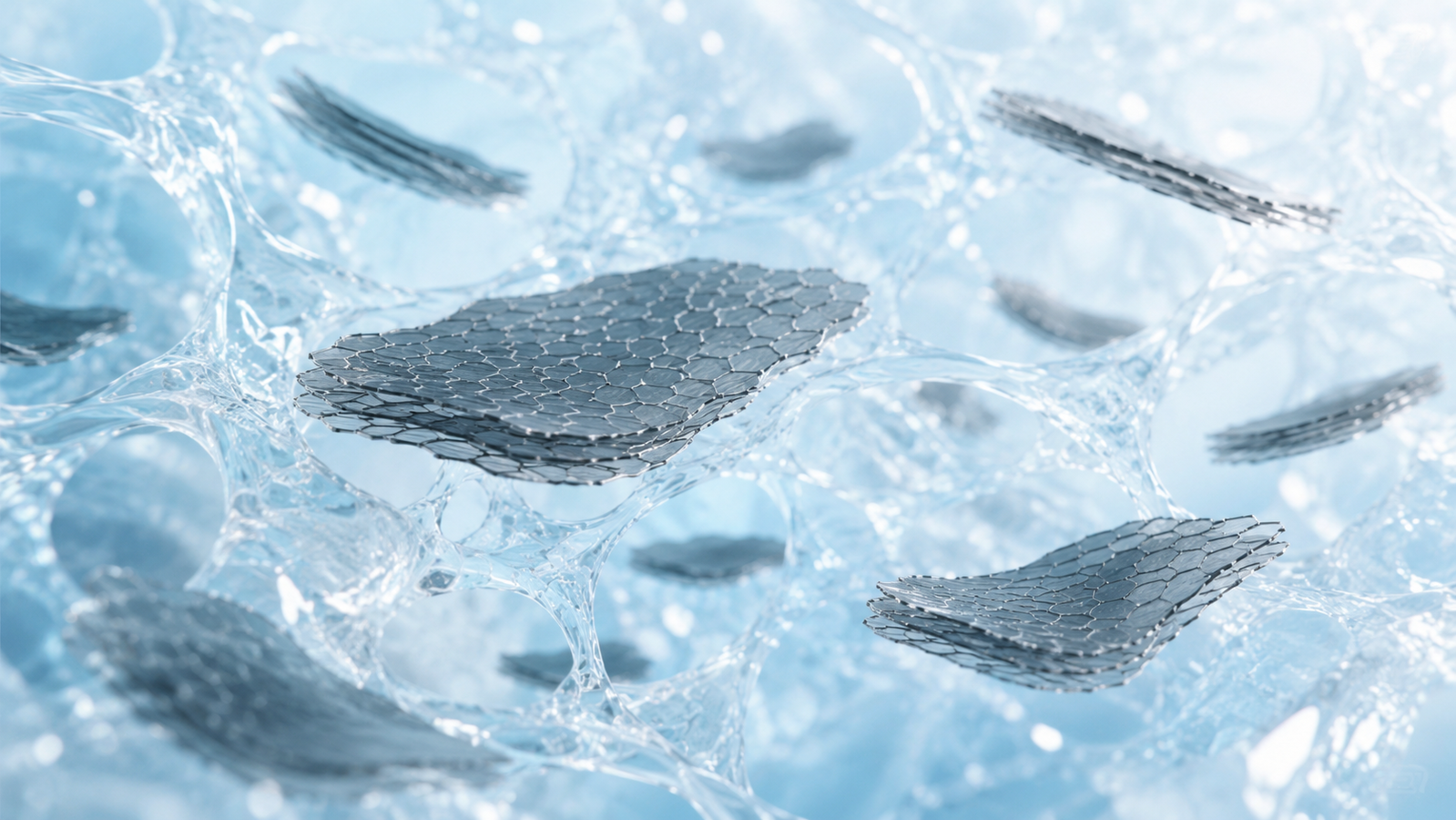
Graphene is a single layer of carbon atoms arranged in a hexagonal, honeycomb lattice — a two-dimensional crystal first isolated from graphite in 2004 by Andre Geim and Konstantin Novoselov, who shared the 2010 Nobel Prize in Physics for the work.1 A graphene nanoplatelet is not a single sheet but a short stack of those sheets: a flat, plate-shaped particle made of a few to a few tens of stacked graphene layers. Crucially, graphene and its platelets are made of pure carbon — an element, not a compound — so older descriptions of graphene as "the thinnest compound" are simply a misnomer.
The single most important point about graphene nanoplatelets is that they are a family, not one fixed specification. Commercial grades range from very thin platelets of only a handful of layers (on the order of 1–2 nm) up to thicker stacks of tens of nanometers, with lateral flake sizes from well under a micron to tens of microns. This breadth is recognized in the field's recommended nomenclature, which classifies two-dimensional carbons by layer number, lateral dimension, and chemical modification rather than lumping them under one label.2 An older claim that graphene nanoplatelets simply "have an average thickness of 1–2 nm" describes one thin grade, not the category as a whole.
What ties the family together is morphology. Each platelet is extremely thin relative to its width, giving a high aspect ratio — the ratio of lateral size to thickness, often in the hundreds or thousands. That flat, high-aspect-ratio geometry is the reason a small amount of material can reach across a composite, block diffusing molecules, bridge into conductive networks, and carry mechanical load far more efficiently than compact particles. Everything else in this guide follows from that shape.
GnP vs Graphene, Graphene Oxide & Graphite
It helps to place graphene nanoplatelets among their relatives, because the distinctions are often blurred — including in older marketing copy.
Single-layer graphene is one isolated sheet: the benchmark for properties, with a Young's modulus near 1 TPa and intrinsic strength around 130 GPa,3 but expensive and difficult to produce and handle at scale — which is why platelets, not single sheets, dominate real-world use.4,5 Graphene nanoplatelets trade a little of that ideal performance for manufacturability: stacking a few layers makes the material far cheaper to produce in bulk and far easier to disperse, while retaining most of the in-plane stiffness, conductivity, and impermeability that matter in a composite.
Graphite sits at the other end: thousands of stacked layers, a bulk mineral. A graphene nanoplatelet is best thought of as a fragment of graphite thin enough to behave two-dimensionally; as platelets get thicker, their behavior trends back toward that of fine graphite. Graphene oxide (GO) is a different branch entirely — graphene sheets chemically decorated with oxygen groups, which makes GO water-dispersible and an electrical insulator until it is reduced.6 GnP, by contrast, are largely unfunctionalized carbon and are conductive as made.
One legacy claim deserves direct correction: it is sometimes said that graphene nanoplatelets have "better barrier properties than graphene" and that "plain graphene can't be dispersed." Both are misleading. Defect-free single-layer graphene is itself an essentially perfect gas barrier — impermeable even to helium.7 The practical advantage of GnP is not that a platelet blocks gas better than graphene does, but that platelets disperse into a matrix and create a long, winding diffusion path; and graphene-family materials can in fact be dispersed by a range of routes, from liquid-phase exfoliation to chemical functionalization.8,9 Dispersibility is a matter of degree and method, not a yes/no line between graphene and its platelets.
Structure & Key Properties
Inside a platelet, the layers are spaced about 0.335 nm apart — the interlayer distance of graphite. So a platelet's thickness follows directly from its layer count: roughly n×0.335 nm for n layers. A 1–2 nm grade is therefore only about three to six layers thick; a 10 nm platelet is roughly thirty. The simulator below makes this concrete — set the number of layers and watch the thickness, the regime (monolayer, few-layer, or thicker nanoplatelet), and the surface area respond.
Surface area is one of the most consequential — and most misunderstood — numbers. A single isolated graphene sheet has a theoretical specific surface area of about 2630 m²/g, because both of its faces are exposed. The instant sheets stack, the internal faces are buried, so the accessible area of an n-layer platelet falls roughly as 1/n. Thinner grades thus offer more surface per gram, which is why they tend to need less material to reach a given effect; the trade-off is that very thin, high-area platelets are also the hardest to disperse without re-stacking. Measured BET surface areas are always lower than the theoretical ceiling and depend on lateral size, defect density, and how completely the powder has been exfoliated.
The in-plane properties that GnP inherit from graphene are exceptional. Graphene's intrinsic strength is about 130 GPa and its Young's modulus near 1 TPa3 — figures that refer to a defect-free single sheet, not to a bulk platelet or a composite, so they should never be quoted as the tensile strength of a finished part. Graphene also conducts heat exceptionally well, with reported single-layer thermal conductivities in the thousands of W/m·K,10 and it is a strong electrical conductor with high carrier mobility.11 A point worth correcting from older overviews: a single graphene sheet is not easily seen with the naked eye — it absorbs only about 2.3% of visible light per layer, a value set by the fine-structure constant, and becomes visible only through interference on specific substrates or when stacked into thicker platelets.12
How GnP Are Made
Because graphite is just stacked graphene held together by weak van der Waals forces, most routes to graphene nanoplatelets are top-down: start with graphite and pull the layers apart far enough to behave two-dimensionally, without fully separating every sheet.
Liquid-phase and ultrasonic exfoliation. Graphite is dispersed in a solvent or surfactant solution whose surface energy matches that of graphene, and ultrasonic or shear energy peels the stack into few-layer platelets. This balance of solvent–graphene interaction against the energy needed to exfoliate is what makes the method work, and it can yield defect-free few-layer material in usable quantities.8 ACS Material's thinnest grade is produced by ultrasonic exfoliation, which favors very thin platelets.
Mechanical and interlayer cleavage. Controlled milling, intercalation, and cleavage processes split graphite into thicker few-layer platelets at higher throughput; these routes underpin many mid-range and industrial grades, where slightly thicker flakes are acceptable in exchange for cost and volume.
Oxidation–reduction. A separate family of routes oxidizes graphite to graphene oxide, exfoliates it in water, then chemically or thermally reduces it back toward graphene (reduced graphene oxide).6 This is the most scalable, lowest-cost path to graphene-like powder, though the product carries residual defects and oxygen and is usually classed as rGO rather than pristine GnP. The choice of route sets the grade: exfoliation gives cleaner, more conductive platelets; oxidation–reduction gives the highest volumes at the lowest cost.
How GnP Are Characterized
No single measurement defines a graphene nanoplatelet; suppliers and researchers combine several. Raman spectroscopy is the fastest fingerprint: the relative intensities of the D, G, and 2D bands report on layer number, disorder, and defect density, and the technique is sensitive enough to distinguish single-, few-, and many-layer material.13 Electron microscopy (TEM/SEM) images flake shape, lateral size, and edges, while atomic force microscopy (AFM) measures thickness directly by scanning the platelet height. X-ray diffraction (XRD) probes interlayer spacing and stacking, and BET gas adsorption gives the specific surface area that correlates with effective thickness.
Why GnP Improve Composites: Barrier, Conductivity, Strength
The headline use of graphene nanoplatelets is as a multifunctional filler. A single additive can improve several properties at once — reducing the need for separate barrier films, conductive additives, and reinforcing fibers.9,14 Each benefit traces back to the platelets' flat, high-aspect-ratio shape, and each has its own mechanism worth seeing directly.
Gas barrier: the tortuous path. Because each platelet is impermeable, a gas molecule cannot cross it — it has to detour around. Pack a matrix with wide, well-aligned platelets and a short straight path through the film becomes a long, winding one. The Nielsen model captures this for aligned platelets: relative permeability falls roughly as (1−φ) / (1 + (α/2)φ), where φ is the volume fraction and α the aspect ratio, so even a few volume percent of high-aspect-ratio flakes can cut gas transport several-fold.15 Adjust the aspect ratio and loading below and watch the path — and the permeability — change.
Electrical conductivity: percolation. Isolated platelets in an insulating matrix carry no current across the sample; charge has to hop from flake to overlapping flake. As loading rises, the flakes touch more and more until, at a critical loading called the percolation threshold, one connected cluster suddenly bridges the whole sample and conductivity jumps by orders of magnitude.16,17 High-aspect-ratio platelets reach that threshold at low loadings, which is exactly why thin, wide graphene nanoplatelets are such efficient conductive and antistatic fillers. Drag the loading slider below to build the network and watch conductivity switch on.
Mechanical reinforcement. Graphene is roughly a thousand times stiffer than a typical polymer, so when platelets are well bonded and aligned, stress transfers from the soft matrix into the rigid flakes and the composite resists deformation.18 The Halpin–Tsai model estimates the stiffness gain from the filler modulus, the aspect ratio, and the loading — and it shows clearly that long, thin platelets reinforce far more effectively per unit mass than compact particles.19 The simulator below compares a neat matrix against a platelet-filled composite under the same pull.
Thermal transport. The same conductive, high-aspect-ratio networks that carry charge also carry heat, and graphene nanoplatelets are widely used to raise the thermal conductivity of polymers and compounds for heat-management parts.10,20 As with electrical percolation, connected platelet pathways and good interfacial contact matter more than loading alone. Graphene-family fillers can also act as nucleating agents that change how the matrix crystallizes, feeding back into the final mechanical and barrier behavior.21
Applications
The multifunctional nature of graphene nanoplatelets puts them across a broad span of industries, in line with the broad application roadmap long projected for graphene materials.22
Composites and lightweighting. GnP-reinforced plastics, rubbers, and other matrices gain stiffness, strength, and surface hardness at low weight, attractive to automotive, aerospace, and construction where reducing mass improves efficiency.18,23,24 Energy and power. Platelets are used in battery electrodes, supercapacitors, and fuel-cell components, where their conductivity and surface area improve rate capability, durability, and capacity, often at low cost.25 Conductive inks and coatings. GnP-loaded inks and coatings give printed electronics, RFID antennas, heat sinks, smart packaging, and antistatic layers their electrical and thermal performance. EMI shielding and thermal management. Connected platelet networks both reflect and dissipate, making GnP composites useful for electromagnetic-interference shielding and for spreading heat away from electronics.20,26 Across all of these, the recurring theme is that one filler delivers several functions at once.
Choosing the Right Grade
Because GnP are a family, picking a grade means matching thickness and lateral size to the job rather than asking for "graphene nanoplatelets" in the abstract.
Thinner platelets (fewer layers, higher surface area, higher aspect ratio) are the most graphene-like: they percolate at lower loadings, build barrier and conductivity efficiently, and suit electronics, sensors, and applications where performance per gram matters — but they cost more and demand more care to disperse without re-stacking. Thicker platelets trade some surface area and aspect ratio for lower cost and easier handling, and are well suited to bulk structural composites and high-volume compounds. Lateral size matters independently of thickness: larger flakes raise aspect ratio (good for barrier and low-loading conductivity) but can be harder to disperse uniformly and may not fit thin coatings. The practical path is to start from the property you need — barrier, conductivity, stiffness, or thermal — and let the required aspect ratio and loading point you to a grade.
Handling, Dispersion & Storage
Dispersion quality, more than raw loading, usually decides how a GnP composite performs — poorly dispersed, re-stacked platelets behave like small lumps of graphite and squander the aspect ratio you paid for. Platelets are blended into liquids, solvents, and polymer melts using sonication, high-shear mixing, three-roll milling, or in-situ polymerization; surfactants or compatibilizers and, for some systems, mild functionalization help wet the flakes and keep them apart.9,14 As noted above, dry-powder agglomerates can partially break down under shear, but complete single-flake dispersion is rarely achieved and is not always necessary — the goal is a well-distributed, connected network appropriate to the property you want.
As fine, low-density powders, graphene nanoplatelets should be handled with appropriate dust precautions and stored sealed, away from light, at normal temperature, following the supplier's safety data sheet. Keeping the powder sealed until use limits moisture pickup and contamination.
ACS Material Graphene Nanoplatelet Products
ACS Material supplies graphene nanoplatelets across the thickness range described above, so you can match a grade to your aspect-ratio and loading targets:
- Graphene Nanoplatelets (1–2 nm) — the thinnest grade, roughly three to six layers, with lateral sizes around 2–3 µm and the highest expected surface area; produced by ultrasonic exfoliation for the lowest conductive loadings and the most graphene-like behavior.
- Graphene Nanoplatelets (1–5 nm) — a thin, high-aspect-ratio grade balancing surface area against easier handling.
- Graphene Nanoplatelets (2–10 nm) — a versatile mid-range grade with lateral sizes around 2–7 µm, produced by interlayer cleavage; a practical default for many composite, conductive, and thermal applications.
- Industrial Thin-Layer Graphene Nanoplatelets — higher-volume grades for bulk composites and compounding where cost and throughput lead.
- Full graphene nanoplatelet range — including fluorinated and specialty grades; see the series page for the complete catalog and specifications.
Each product page lists the specifications, characterization data, and safety documentation for that grade. If you are unsure which grade fits your target property and loading, our team can help you match material to application.
Frequently Asked Questions
What are graphene nanoplatelets?
Graphene nanoplatelets (GnP) are small, plate-shaped stacks of a few to a few tens of graphene layers — thin enough to keep much of graphene's stiffness, conductivity, and impermeability, but far cheaper to produce and easier to disperse than single-layer graphene. They are commercially accessible graphene-family materials available from suppliers in a range of thicknesses and lateral sizes.
How thick are graphene nanoplatelets?
There is no single thickness — that is the key point. Layers sit about 0.335 nm apart, so thickness is roughly the layer count times 0.335 nm. Commercial grades run from a few layers (around 1–2 nm) to tens of nanometers, with lateral sizes from under a micron to tens of microns. Quoting a single "1–2 nm" figure describes only one thin grade.
What are graphene nanoplatelets used for?
Mainly as a multifunctional filler. Adding a few volume percent to a plastic, rubber, coating, or electrode can raise stiffness and strength, switch on electrical conductivity, cut gas permeation, improve thermal conductivity, and provide EMI shielding — often several at once. That puts them in composites, batteries and supercapacitors, conductive inks, antistatic and barrier coatings, and thermal-management compounds.
How do you disperse graphene nanoplatelets?
Platelets are dispersed into liquids, solvents, and polymer melts using sonication, high-shear mixing, three-roll milling, or in-situ polymerization, often with surfactants or compatibilizers. Dispersion quality usually matters more than loading: well-separated platelets build efficient networks, while re-stacked ones behave like graphite. Complete single-flake separation is rarely necessary — a well-distributed, connected network is the goal.
Are graphene nanoplatelets the same as graphene?
No. Single-layer graphene is one isolated sheet and the benchmark for properties; a nanoplatelet is a stack of several layers. The platelet gives up a little ideal performance in exchange for being much cheaper to make and far easier to disperse, which is why GnP, not single-layer graphene, are what most industries actually use.
How are graphene nanoplatelets different from graphene oxide?
Graphene oxide (GO) is graphene chemically decorated with oxygen groups, which makes it water-dispersible but electrically insulating until it is reduced. Graphene nanoplatelets are largely unfunctionalized carbon and are conductive as made. GO is favored where water processing and chemical tunability matter; GnP where conductivity and mechanical reinforcement matter.
Is graphene a metal or a plastic?
Neither. Graphene is a pure-carbon material — an allotrope of carbon — and is best described as a semimetal because of its electronic structure and high conductivity.
What does the particle size on a datasheet mean?
Be careful here: a powder particle-size distribution (D10/D50/D90) measured by laser diffraction usually reflects loosely bound agglomerates, which can be tens of microns even when individual flakes are only a few microns across. Single-flake lateral size and powder PSD are different numbers; agglomerates can partially break apart during compounding depending on shear and formulation.
References
This article is provided by ACS Material LLC for educational purposes and describes graphene nanoplatelets. Some property values cited — such as the stiffness, strength, transparency, and surface area of an ideal single sheet — refer to idealized or single-layer graphene and the specific studies referenced; a multilayer platelet, or any real composite, will fall short of these figures, and actual performance depends on grade, dispersion, alignment, and formulation. Consult product datasheets and safety data sheets for grade-specific specifications and handling guidance. Interactive simulators are schematic teaching tools based on the stated models, not predictive design software.