
A mask aligner prints a photomask 1:1 into photoresist, and the distance between mask and resist decides how fine the pattern can be. This guide explains the exposure modes, how to estimate resolution from the gap and the wavelength, what creates gaps nobody intended, and how the lamp, the dose and the substrate enter the result.
In one paragraph: Closer mask-to-resist spacing generally improves resolution, while a proximity gap can protect the mask and accommodate substrate topography [1]. The estimate d ≈ (λg)1/2 gives roughly 1.9 µm at 365 nm and a 10 µm gap, but it is not a guaranteed process resolution [1]. Particles, bubbles, mask contamination, substrate shape and edge beads can create unintended gaps [1][4]. Measure intensity at the wavelength relevant to the dose, convert dose to time with t = D/I, and qualify the exposure process with an exposure series [1].
1. What a Mask Aligner Does
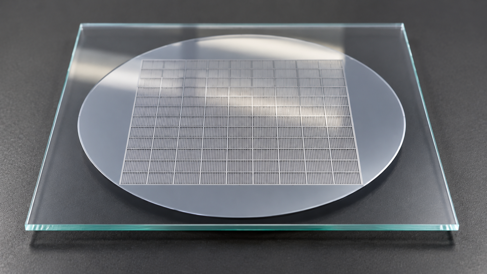
A mask aligner transfers the pattern of a photomask into a photoresist film by exposing it through the mask with near-parallel ultraviolet light. The structures on the mask correspond 1:1 to the exposed areas of the resist; there is no reduction optics [1]. That simplicity is why mask aligners are standard tools in research and pilot lines. It also means that what limits resolution is mostly the geometry between mask and resist, not a lens [1][3].
MicroChemicals notes that the best resolution is reached when the mask and the resist surface are in direct contact, whereas textured substrates, for example, may need a gap between the mask and the resist [1]. Other exposure routes exist: a stepper projects the mask through reduction optics, and laser direct writing needs no mask at all [1]. This guide stays with the mask aligner and explains:
- what the exposure modes change, and why a gap reduces resolution;
- how to estimate the smallest feature for a given gap and wavelength;
- what creates gaps nobody intended, from particles to edge beads;
- how the lamp, the dose and the substrate enter the result.
Where this sits in the wider family of thin-film methods is explained in Solution-Processed Thin Films: Choosing Spin, Dip, Slot-Die or Blade Coating. Coating the resist itself is the topic of Photoresist Spin Coating: From Viscosity to Target Thickness and Uniformity.
2. Contact, Vacuum, Soft and Proximity Modes
Mask aligners usually offer several ways of bringing the mask and the substrate together. The names describe how close, and how firmly, the mask and the resist surface meet. Exact definitions, forces and vacuum levels differ between instruments, so the instrument manual is the reference; in general use:
| Mode | Mask and resist | Typical reason to choose it |
|---|---|---|
| Vacuum contact | Mask and substrate pulled together by evacuating the space between them; the closest contact | Finest features on flat, clean substrates |
| Hard contact | Substrate pressed against the mask | Fine features where vacuum contact is not needed or not possible |
| Soft contact | Substrate brought against the mask with less force | Less mechanical load on mask and resist, with some loss of intimacy of contact |
| Proximity | A defined gap is left between mask and resist | Protecting the mask, textured or fragile substrates, avoiding sticking |
General descriptions of common exposure modes; the resolution-versus-gap trade-off follows MicroChemicals [1], which does not define the individual contact modes. Contact forces, vacuum levels and gap settings are instrument-specific and must be confirmed in the instrument documentation.
The trade-off runs in one direction. Closer contact gives better resolution, because diffraction has less distance in which to blur the image [1][3]. A gap protects the mask and the resist. MicroChemicals lists two reasons for an intended gap: to prevent damage to the mask on textured substrates, and on smooth substrates to stop the mask sticking to the resist film [1].
Contact also has a practical side. Particles or resist residues on the mask are one of the causes of unintended gaps that MicroChemicals lists [1], and a contaminated mask carries the problem to every following substrate. Labs that run many contact exposures therefore inspect and clean masks routinely.
3. How the Gap Sets Resolution
The openings in a photomask are often only a few to a few tens of exposure wavelengths wide. The light passing them is therefore not a perfect parallel image but a diffraction pattern, treated like diffraction at a single slit [1]. MicroChemicals gives the attainable lateral resolution d on the resist surface as [1]:
λ = exposure wavelength; g = gap between the underside of the mask and the resist surface. Single-slit estimate as given by MicroChemicals [1].
Two things follow. Resolution improves only with the square root of the gap, so halving the gap gains about 30 %, not 50 %. And shorter wavelengths help, which is one reason the i-line at 365 nm is common for fine work [1].
| Gap g | d at 365 nm (i-line) | d at 435 nm (g-line) |
|---|---|---|
| 1 µm | about 0.6 µm | about 0.66 µm |
| 5 µm | about 1.35 µm | about 1.47 µm |
| 10 µm | about 1.9 µm | about 2.1 µm |
| 20 µm | about 2.7 µm | about 2.95 µm |
| 50 µm | about 4.3 µm | about 4.7 µm |
Arithmetic from d ≈ (λg)1/2 [1]. An estimate of the order of magnitude, not a guaranteed resolution; resist, process and mask quality decide what you actually resolve.
A textbook estimate with resist thickness
Lithography textbooks also give a gap-and-resist-thickness estimate for the minimum period of a line-space grating, commonly written as 2bmin ≈ 3 · [λ(s + z/2)]1/2, where s is the mask-to-resist gap and z is resist thickness [2][3]. This estimates a different feature metric from the simpler d ≈ (λg)1/2 expression above. Treat both as approximate diffraction-based guides, not interchangeable specifications or guarantees of printed resolution.
The simple estimate falls to zero at zero gap, but diffraction does not. MicroChemicals notes that even in perfect contact the intensity on the resist surface is not homogeneous, because the opening itself forms a diffraction pattern immediately behind it. In addition, resist near the substrate is further from the mask and sees a more pronounced diffraction pattern, and Rayleigh scattering in the film spreads light sideways [1]. Thinner resist therefore helps resolution in contact printing, within the limits the later process allows.
4. Unintended Gaps: Particles, Bubbles and Edge Beads
Most resolution problems on a mask aligner come from gaps nobody planned. MicroChemicals lists the usual causes [1]:
| Cause of an unintended gap | Where it comes from | What to check |
|---|---|---|
| Particles in the resist film | Clean room air, contaminated substrates, expired resist | Filtered resist, cleaning, clean storage |
| Air bubbles in the resist film | Manual dispensing, too short a waiting time after moving resist containers | Dispense technique, rest time before use |
| Contaminated mask | Particles or resist residues on the mask | Mask inspection and cleaning |
| Substrate shape | Rough, textured or curved (strained) substrates | Flatness, mounting, a planned proximity gap |
| Resist edge bead | Thick resist at the substrate edge | Edge bead removal or reduction |
| Mask orientation | Mask attached upside-down | Chrome side towards the resist |
Causes as listed by MicroChemicals [1]; the checks are general practice.
A gap of a few micrometres from a particle or bubble is enough to move the resolution in the table above by a micrometre or more. Bubbles and particles also show up in the coated film as comets; causes and fixes are covered in Spin Coating Defects: Comets, Striations, Pinholes and Edge Beads Diagnosed.
The edge bead as a spacer
The edge bead deserves its own mention. During coating of thick films and on square substrates, the resist rises at the edge [4]. Because the bead keeps a high residual solvent content even after the softbake, the mask may stick to the resist. The bead also acts as an unwanted spacer between mask and resist, which MicroChemicals names as a frequent reason for poor resolution, wrong dimensions or an unintentionally low sidewall angle [4]. Removing it is described in Edge Bead Removal and Backside Rinse: EBR/BSR in Spin Processing.
5. Lamp, Intensity, Dose and Substrate
A mercury lamp used in mask alignment can emit the g-, h- and i-lines at 435, 405 and 365 nm, plus a weaker continuum [1]. For a 6-inch mask aligner with a 350 W lamp, MicroChemicals gives typical values of about 15–30 mW/cm² overall, with the i-line contributing roughly 40 % [1]. These are source-specific example values, not specifications for the MA200-BE. Two practical consequences:
- Know what your meter measures. Many detectors measure only the i-line, typically 6–12 mW/cm² for such a lamp, so a dose read from an i-line meter is not the same number as the dose over all lines [1].
- Recalibrate. Lamp intensity changes with age, so the intensity should be checked periodically; for non-critical work MicroChemicals suggests that the lateral variation of intensity should stay below about 10 % [1].
For positive and image reversal resists the photoreaction is usually a one-photon process, so dose (intensity multiplied by time) is the main exposure variable; at high intensity, thick films can still be damaged by heat and gas released during exposure [1]. The conversion is:
D = dose (mJ/cm²); I = intensity (mW/cm²); t = exposure time (s). For example, 120 mJ/cm² at 20 mW/cm² needs 6 s.
The substrate also takes part. Light that passes the resist is partly reflected back into it: MicroChemicals gives roughly 10 % for glass, 30 % for silicon and more than 90 % for metal films [1]. The same nominal dose therefore acts more strongly on a metal-coated substrate than on glass. UV-transmitting substrates such as quartz, glass or polymer films bring another effect: they conduct light laterally and allow reflections from the substrate holder, which reduces the lateral resolution and the edge steepness of the developed structures [1].
How to find the right dose with an exposure series, and how development then turns the latent image into a pattern, is covered in Exposure Dose and Puddle Development: Reading a Resist Contrast Curve.
6. A Checklist for the Best Resolution
For the best result from a mask aligner, work through the chain in order:
- Choose the mode for the substrate. Vacuum or hard contact for the finest features on flat substrates; proximity where the mask or the substrate needs protection.
- Estimate the resolution. Use d ≈ (λg)1/2 to check whether the planned gap is plausible for your smallest feature [1].
- Keep the resist thin enough. Thickness adds distance, even in contact [1][2].
- Remove unintended gaps. Clean substrates and masks, bubble-free resist, no edge bead, chrome towards the resist [1][4].
- Calibrate the dose. Measure intensity at the right wavelength, recalibrate periodically and convert dose to time with t = D/I [1].
- Run an exposure series for every new resist, substrate or thickness, and develop under fixed conditions [1].
Thermal steps before and after exposure, such as the softbake and the post-exposure bake for chemically amplified resists, are covered in Soft Bake, Post-Bake and Annealing on a Hot Plate: What Each Step Does.
7. Levon™ Mask Aligner
The table quotes the Levon™ mask aligner product page; “Not stated” means the page does not give the value.
| Specification | MA200-BE |
|---|---|
| Exposure central wavelength | 365 nm |
| Exposure area | 8-inch |
| Exposure resolution | 0.8–1.2 µm |
| Exposure irradiance | >30 mW/cm² (adjustable) |
| Illuminance uniformity | ≤2% over a 4-inch area; ≤3% over an 8-inch area |
| Exposure settings | 0–999.9 s |
| Selectable exposure modes | Hard contact, soft contact, proximity and vacuum contact |
| Registration accuracy | 0.5 µm |
| Relative travel range (wafer to mask) | X, Y: ±5 mm; θ: ±6° |
| Alignment system | Optical microscope + high-definition CCD; magnification 150X–720X, adjustable |
| Leveling and focusing | Auto-leveling and auto-focusing mechanisms |
| Supported reticle sizes | 5″ × 5″, 7″ × 7″, 9″ × 9″ |
| Maximum allowable working thickness (design) | 0.1–3 mm (customizable fixtures supported); wafer fragment handling |
| Proximity gap range | Not stated |
Specifications as published on the Levon™ product page on 22 October 2026. The page gives the exposure resolution without stating the mode, resist or process conditions; the supplied configuration is confirmed in the quotation.
How this connects to the guide: the MA200-BE exposes at a central wavelength of 365 nm, the i-line used for the resolution estimates in Section 3. Its page lists hard contact, soft contact, proximity and vacuum contact as selectable modes, the choice discussed in Section 2; the page does not state the proximity gap range, so ask for it if you plan proximity work. Exposure time is set from 0 to 999.9 s and the irradiance is given as greater than 30 mW/cm² and adjustable; with a measured irradiance, the dose arithmetic of Section 5 gives the exposure time. Alignment uses an optical microscope with an HD CCD at 150X–720X. Questions about a specific configuration can be sent through the contact form.
8. Keep Exploring the Lithography Knowledge Hub
Start here
- Solution-Processed Thin Films: Choosing Spin, Dip, Slot-Die or Blade Coating — thin-film coating methods compared
- Spin Coating Defects: Comets, Striations, Pinholes and Edge Beads Diagnosed — comets, bubbles and other coating defects
Lithography steps
- Photoresist Spin Coating: From Viscosity to Target Thickness and Uniformity — coating the resist to target thickness
- Soft Bake, Post-Bake and Annealing on a Hot Plate: What Each Step Does — softbake and post-exposure bake
- Exposure Dose and Puddle Development: Reading a Resist Contrast Curve — exposure dose and development
- Edge Bead Removal and Backside Rinse: EBR/BSR in Spin Processing — edge bead removal and backside rinse
Links will be added as each article is published.
Equipment
- MA200-BE Mask Aligner — 365 nm, 8-inch exposure area, four exposure modes; published resolution 0.8–1.2 µm, mode and process conditions not stated
- Levon™ Mask Aligners — all mask aligners
Questions about a specific mask aligner can be sent through the contact form.
9. FAQ
Does contact or proximity exposure give better resolution?
Closer contact generally reduces gap-related diffraction blur. Proximity exposure trades some resolution for mask protection or clearance over topography; the best mode depends on the substrate, mask and process [1].
How do I estimate resolution for a given gap?
Use d ≈ (λg)1/2: at 365 nm, a 10 µm gap gives roughly 1.9 µm [1].
Why is my contact exposure resolution poor?
Usually an unintended gap: particles, bubbles, a contaminated mask, a curved substrate, an edge bead or an upside-down mask [1].
Does resist thickness affect resolution?
Yes. Resist near the substrate is further from the mask, so thickness adds distance even in perfect contact [1][2].
How do I convert exposure dose to time?
Divide dose by intensity: t = D/I. 120 mJ/cm² at 20 mW/cm² needs 6 s [1].
Why does my meter read lower than the lamp intensity?
Many meters measure only the i-line, which in MicroChemicals’ 350 W, 6-inch aligner example is roughly 40 % of the g-, h- and i-line output [1].