
Graphene and carbon nanotubes are the two superstars of carbon nanotechnology, and they are intimately related: a carbon nanotube is, quite literally, a sheet of graphene rolled into a seamless cylinder. Yet that single act of rolling — going from a flat two-dimensional sheet to a one-dimensional tube — reshapes their electronic behavior, their ideal applications, and even how they are made. This guide compares graphene and carbon nanotubes (CNTs) head to head: structure, electrical, mechanical, thermal, and optical properties, how each is synthesized, where each one wins, and how to choose between them.
Short answer: graphene is a flat, one-atom-thick 2D sheet of carbon; a carbon nanotube is that same sheet rolled into a 1D cylinder. The deepest difference is electronic: graphene is always a zero-gap semimetal (it conducts superbly but has no natural band gap), whereas a carbon nanotube is either metallic or semiconducting depending on its chirality — the precise angle and diameter at which the sheet is rolled — with roughly one in three tubes metallic and the rest semiconductors with a usable band gap. Both are about ~1 TPa stiff, exceptionally strong, and among the best heat conductors known. In practice, graphene shines as transparent, flexible films and coatings, while CNTs shine as high-strength fibers, composite reinforcement, and transistor channels. They are complementary, not rivals.
| Property | Graphene | Carbon nanotubes (CNTs) |
|---|---|---|
| Dimensionality | 2D sheet, one atom thick | 1D cylinder (a rolled sheet) |
| Electronic type | Zero-gap semimetal (always) | Metallic or semiconducting — set by chirality |
| Electron mobility | Ultrahigh (>100,000 cm² V⁻¹ s⁻¹, suspended) | Very high in semiconducting tubes |
| Young’s modulus | ~1 TPa | ~1 TPa |
| Intrinsic strength | ~130 GPa (strongest measured) | ~11–60 GPa (tube or rope) |
| Thermal conductivity | ~2,000–5,000 W m⁻¹ K⁻¹ | ~3,000–6,000 W m⁻¹ K⁻¹ |
| Optical signature | ~2.3% absorption per layer; transparent | Sharp, chirality-specific absorption |
| Typical form | Films, flakes, coatings, dispersions | Powders, fibers, networks, inks |
| Best-fit uses | Transparent/flexible electrodes, sensors, coatings | Composites, fibers, transistors, field emitters |
What are carbon nanotubes?
Carbon nanotubes are tiny cylinders of carbon, their walls a single hexagonal lattice of carbon atoms. They were brought to wide attention by Sumio Iijima in 1991, who observed needle-like helical microtubules of graphitic carbon in an arc-discharge deposit.1 Two years later, the thinnest possible version — the single-walled carbon nanotube, only about one nanometer across — was reported independently by Iijima and Ichihashi2 and by Bethune and colleagues.3
There are two main families. A single-walled carbon nanotube (SWCNT) is one graphene sheet rolled into a cylinder; a multi-walled carbon nanotube (MWCNT) is several concentric cylinders nested inside one another. Either way, the carbon–carbon bonding makes carbon nanotubes exceptionally strong for their weight — far stronger than conventional structural metals, though real composites depend on tube quality, alignment, and dispersion — and, as we will see, electrically they can behave either as a metal or as a semiconductor depending on exactly how the sheet is rolled.
What is graphene?
Graphene is a single layer of carbon atoms arranged in a two-dimensional honeycomb lattice — the thinnest material known, just one atom thick. Although it is the conceptual building block of graphite, isolating a single free-standing sheet was only achieved in 2004, when Novoselov, Geim and colleagues separated and electrically characterized atomically thin carbon films,4 work that led to the 2010 Nobel Prize in Physics. The properties that followed — record strength, superb conductivity, near-perfect transparency — were soon catalogued in a landmark review.5
Graphene is the parent structure of the other graphitic carbons: stack the sheets and you get graphite, roll one up and you get a carbon nanotube, wrap one into a ball and you get a fullerene. If you want the full background on the 2D sheet itself, see our complete guide to graphene.
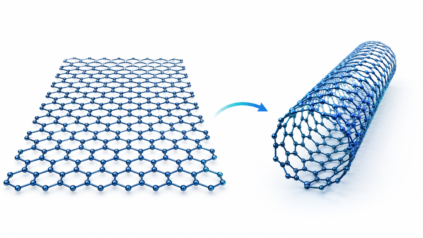
Structure: a nanotube is a rolled sheet
The relationship between the two materials is not just an analogy — it is geometric. Take a graphene sheet and roll it up, and you have a nanotube. The direction in which you roll is captured by two integer indices, written (n, m), called the chiral indices. Together they fix the tube’s diameter and its “twist,” or chiral angle. Three special cases have names: armchair tubes (where n = m), zigzag tubes (where m = 0), and chiral tubes (everything in between).
Crucially, those indices do far more than set the geometry. As early as 1992, theory by Hamada and colleagues6 and by Saito and colleagues7 predicted that the way a sheet is rolled decides whether the resulting tube conducts like a metal or behaves like a semiconductor. Graphene, by contrast, is always the same flat sheet with a single electronic identity. This is the root of nearly every practical difference between the two materials.
Electrical properties: the deepest difference
Electrically, graphene and carbon nanotubes diverge more than anywhere else. Graphene is a zero-gap semimetal: its valence and conduction bands meet at single points (the Dirac points), so its charge carriers behave like massless particles and move with extraordinary mobility — exceeding 100,000 cm² V⁻¹ s⁻¹ in clean, suspended samples.8 That makes graphene a superb conductor. But the absence of a band gap means a graphene transistor cannot be switched fully off, which is a problem for digital logic.
Carbon nanotubes solve this in a way graphene cannot. A tube is metallic or semiconducting depending purely on its chirality. The rule — predicted by Mintmire,9 Hamada,6 and Saito7 — is that a tube is metallic when (n − m) is divisible by three, and semiconducting otherwise. So about one third of all possible tubes are metals and two thirds are semiconductors. Scanning tunneling microscopy by Wildoer and colleagues10 and by Odom and colleagues11 confirmed this directly, imaging a tube’s atomic structure and measuring the matching electronic states.
A semiconducting tube has a band gap that scales roughly as the inverse of its diameter — about 0.9 electron-volts divided by the diameter in nanometers — which is exactly what a transistor needs. The first room-temperature transistor built from a single carbon nanotube was demonstrated by Tans, Verschueren and Dekker in 1998,12 and semiconducting tubes were later shown to carry charge with extraordinary mobility.13 Even metallic tubes are remarkable: they act as near-ideal one-dimensional quantum wires.14
The interactive map above lets you dial the indices (n, m) and watch a tube flip between metal and semiconductor while its diameter, chiral angle, and band gap update live. Notice the pattern: the metallic tubes (filled dots) fall on every third diagonal, and the armchair line (n = m) is always metallic. Graphene has no such knob — it is fixed at zero gap. To give graphene a usable band gap, researchers must engineer it (cutting it into narrow nanoribbons, stacking bilayers, or applying strain), usually at the cost of some mobility. A nanotube, by contrast, gets its band gap “for free” from its geometry.
Mechanical strength: both extraordinary
Both materials are built from the same strong carbon–carbon bonds, so both are stiff and remarkably strong. Graphene holds the intrinsic-strength record: nanoindentation of defect-free monolayers gives a Young’s modulus near 1 terapascal and an intrinsic breaking strength around 130 GPa, making it the strongest material ever measured.15
Carbon nanotubes are comparably stiff. Early estimates from the amplitude of their thermal vibrations placed the modulus in the terapascal range,16 single-walled tubes were measured at around 1.25 TPa,17 and direct nanobeam tests confirmed their elasticity, strength, and toughness.18 Under tension, multi-walled tubes break at tens of gigapascals,19 and ropes of single-walled tubes show similar strength.20 The practical distinction is shape: graphene reinforces as a 2D sheet and barrier, while a nanotube acts as a high-aspect-ratio 1D fiber — ideal for bridging cracks and carrying load along its axis in a composite.
Thermal conductivity: heat superhighways
Both materials conduct heat better than copper. Suspended single-layer graphene was measured at roughly 2,000–5,000 W m⁻¹ K⁻¹,21 and the thermal behavior of graphene and related carbon nanostructures has been reviewed in depth.22 Carbon nanotubes are equally impressive: theory predicted values up to around 6,600 W m⁻¹ K⁻¹ for an isolated tube,23 and measurements on individual multi-walled tubes exceeded 3,000 W m⁻¹ K⁻¹.24 Both are therefore prized for thermal management — graphene as a heat-spreading film, nanotubes as conductive fillers and vertical heat paths.
Optical properties
Graphene is famously transparent: a single layer absorbs just 2.3% of visible light, a value set by the fine-structure constant of nature.25 Adding a few layers simply subtracts another ~2.3% each, which is what makes graphene so attractive as a transparent conductor. Carbon nanotubes interact with light very differently: each (n, m) species has sharp, characteristic optical transitions tied to its electronic structure, and structure-assigned spectra let researchers identify exactly which tubes are present in a sample.26 In short, graphene’s optics are broadband and featureless, while a nanotube’s are a fingerprint of its chirality.
How they are made
The two materials are produced by overlapping but distinct routes. Carbon nanotubes were first made by arc discharge — scaled up to bulk quantities by Ebbesen and Ajayan in 199227 — and by laser ablation, which produced highly crystalline ropes of single-walled tubes.28 Today, catalytic chemical vapor deposition (CVD) dominates for bulk powders and for aligned, patterned growth.
Graphene can be peeled directly from graphite — the original mechanical exfoliation,4 which still gives the highest quality — or grown over large areas by CVD: uniform films on copper foil,29 few-layer films on arbitrary substrates,30 patterned films for stretchable transparent electrodes,31 and even roll-to-roll production of 30-inch sheets.32 For solution processing, chemically derived graphene oxide and reduced graphene oxide provide a scalable, ink-compatible path.
Where each one wins
Because of their different shapes, the two materials gravitate toward different jobs. Graphene excels wherever a thin, transparent, conductive, or impermeable layer is needed: flexible and transparent electrodes,31, 32 conductive polymer composites,33 high-surface-area electrodes for supercapacitors and batteries,34 chemical and biological sensors, and barrier coatings.
Carbon nanotubes excel wherever one-dimensional strength and conductivity matter: reinforcing fibers and structural composites, conductive networks and printable inks, transistor channels and interconnects, and field-emission sources — a breadth of applications surveyed early by Baughman and colleagues.35 And as graphene production continues to scale and costs fall, its role across mainstream electronics and energy keeps expanding.36
Hybrids: using both together
The two are not mutually exclusive — in fact, they pair naturally. Combining 1D nanotubes with 2D graphene produces hybrid carbon architectures in which the tubes bridge the gaps between sheets, building continuous, mechanically robust, three-dimensional conductive networks. These graphene–nanotube hybrids are being explored for high-performance electrodes, flexible electronics, and strong lightweight composites, drawing on graphene’s large surface and the nanotube’s length at the same time.
Which should you choose?
Choose graphene when you need a flat, transparent, or high-surface-area conductor: touch panels and flexible displays, EMI shielding and barrier films, supercapacitor and battery electrodes, and chemical or biological sensors. Choose carbon nanotubes when you need one-dimensional reinforcement or a switchable semiconductor: structural and conductive composites, conductive fibers and yarns, transistor channels, and field-emission sources.
A simple rule of thumb: if your goal is a clean, switchable band gap, semiconducting nanotubes have a natural advantage; if your goal is the highest sheet conductivity and optical transparency, graphene leads. For many emerging devices, the best answer is to use both.
ACS Material carbon nanomaterials
- Carbon Nanotubes — single- and multi-walled CNTs in research and bulk grades for composites, electronics, and energy.
- Single-Walled Carbon Nanotubes (SWCNTs) — high-purity SWCNTs for transistors, transparent conductors, and sensing.
- Multi-Walled CNTs (MWCNTs) — robust, conductive multi-walled tubes for reinforcement and conductive networks.
- Graphene Series — single-layer graphene, graphene oxide, rGO, and related grades.
- CVD Graphene — large-area graphene films on copper and target substrates for transparent electrodes, sensors, and device research.
- Graphene Oxide (GO) — hydrophilic, solution-processable graphene oxide for films, coatings, and composites.
Related reading
- Complete Guide to Graphene — structure, properties, production, and applications of the 2D sheet.
- Graphene-like Materials — 2D materials beyond graphene, including black phosphorus, TMDs, MXenes, and hBN.
- Reduced Graphene Oxide in Concrete — rGO and GO as cementitious nanomaterial additives.
Frequently asked questions
Is a carbon nanotube just rolled-up graphene?
Essentially, yes. A single-walled carbon nanotube is a graphene sheet rolled into a seamless cylinder. The direction of rolling — its chirality — then sets the tube’s diameter and whether it behaves as a metal or a semiconductor.
Which is stronger, graphene or carbon nanotubes?
On an intrinsic basis, graphene holds the record, with a breaking strength around 130 GPa.15 Carbon nanotubes are comparably stiff (~1 TPa modulus) and extremely strong as fibers, which makes them especially useful for reinforcing composites along one direction.
Why can carbon nanotubes be semiconductors but graphene cannot?
Graphene’s flat lattice closes its band gap, so it is a zero-gap semimetal. Rolling the sheet into a tube quantizes the electrons around the circumference; depending on the chiral indices (n, m), the allowed states either include or miss the crossing point, making the tube metallic or semiconducting.9, 10
Which is better for transistors?
Semiconducting carbon nanotubes, because they have a real band gap and can be switched fully off.12, 13 Graphene needs extra engineering — nanoribbons, bilayers, or strain — to open a gap, which usually lowers its mobility.
Which is better for transparent electrodes?
Graphene, because a single layer is about 97.7% transparent yet highly conductive, and it can now be grown and transferred over large areas.25, 32
Can graphene and carbon nanotubes be used together?
Yes. Graphene–nanotube hybrids combine the 2D sheet and the 1D tube into conductive, mechanically strong networks used in electrodes, composites, and flexible electronics.
References
This article is provided by ACS Material LLC for educational purposes and compares graphene and carbon nanotubes (CNTs), including single-walled and multi-walled tubes. The property values cited — modulus near 1 TPa, intrinsic strength around 130 GPa, ~2.3% per-layer optical absorption, thermal conductivities of several thousand watts per meter-kelvin, and mobilities above 100,000 cm² V⁻¹ s⁻¹ — refer to idealized, defect-free, or single-structure samples in the referenced studies; real powders, films, fibers, and composites will fall short and depend strongly on grade, purity, chirality distribution, defects, dispersion, and alignment. The interactive chirality map is a schematic teaching tool based on the standard zone-folding model (diameter, chiral angle, the (n − m) mod 3 metallicity rule, and an approximate inverse-diameter band gap), not predictive device-design software. Consult product datasheets and safety data sheets for grade-specific specifications and handling guidance.