
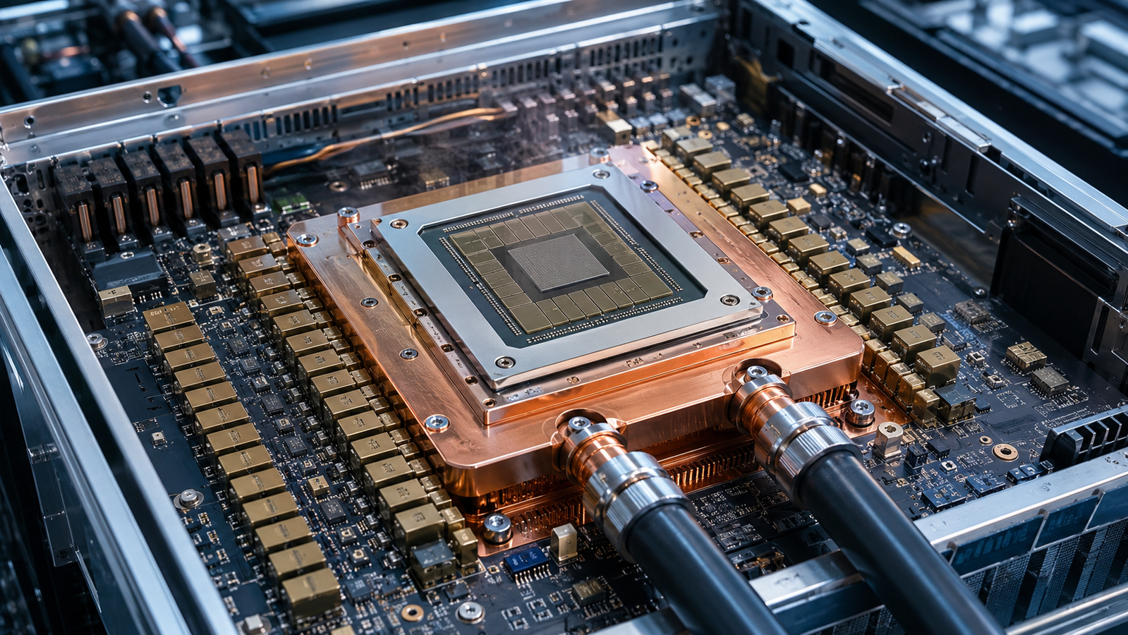
The number that matters is not the kilowatt. Flagship AI accelerators have reached the 1 kW class1, while current infrastructure guidance describes rack densities rising from roughly 120 kW toward several hundred kilowatts, with megawatt-class racks anticipated2. But data centers have always handled megawatts. What they have never handled is this many watts through this little area. Divide 1,000 W by a die a few centimeters on a side and you get a heat flux in the region of 50–100 W/cm² sustained, with local hotspots far higher — a flux regime rarely encountered at package-average scale in mainstream computing. That is the thermal wall, and it is a statement about physics, not about engineering effort. This article quantifies the wall layer by layer — flux, spreading, interfaces, coolant — and ends where every defensible thermal program eventually depends: on measurement.
- 1A kilowatt is not the problem. The square centimeter is
- 2We solved this flux in 1981 - for one chip
- 3The temperature budget: where the kelvins actually go
- 4The wall is moving inward
- 5Put numbers on the wall
- 6Why the wall turned into a materials race
- 7What this means for anyone buying or building thermal hardware
- 8Keep exploring the knowledge hub
A kilowatt is not the problem. The square centimeter is
Heat removal is bookkeeping. At steady state, every watt generated in the die must cross the package boundary, and the difficulty of moving it is set by flux — watts per unit area — not by total power. A 1,000 W package on a 16 cm² lid is a 62 W/cm² problem before any spreading; shrink the effective area, as 3D stacking and chiplet integration do by concentrating dissipation under logic tiles3. Flux is what the cooling stack actually sees.
The reason flux is punishing comes from the simplest equation in heat transfer: q″ = h·(Twall − Tbulk). The heat flux q″ that a surface can reject equals the convective coefficient h of the cooling technology times the temperature difference you can afford. Both factors are bounded. Silicon reliability caps junction temperature; coolant supply temperature is set by the facility; the difference between them — minus everything the package itself consumes — is rarely more than a few tens of kelvin. And h is a property of physical mechanisms, not of ambition: natural convection delivers on the order of 5–25 W·m−2·K−1, forced air over finned heat sinks tens to a couple hundred, single-phase liquid cold plates thousands to tens of thousands, and boiling or microchannel schemes more still. For a specified wetted area and wall-to-fluid temperature difference, q″ = h·(Twall − Tbulk) sets the required local coefficient. In a real package, fins and channels multiply the wetted area, while the die, TIM and spreader consume part of the total junction-to-coolant temperature budget — so the reference h ranges indicate increasing architectural difficulty rather than universal pass/fail limits. Real performance also depends on wetted-area multiplication, flow regime, pressure drop, and how the total junction-to-coolant temperature budget is divided among the die, interfaces4, spreader and fluid film — not on a single coefficient in isolation.
We solved this flux in 1981 — for one chip
The flux numbers alarming the industry today have a famous precedent. In 1981, Tuckerman and Pease etched microscopic water channels directly into the back of a silicon substrate and demonstrated removal of 790 W/cm² with a 71 °C rise above the inlet water — an order of magnitude beyond today’s package-average fluxes, achieved forty-five years ago5. Their insight was structural: for laminar flow in confined channels the convective coefficient scales inversely with channel width, so microscopic channels buy enormous h. Modern research has pushed the same logic further by co-designing the microfluidics with the electronics inside one substrate, demonstrating fluxes beyond 1,700 W/cm² in embedded-cooling test devices6.
So why is there a wall at all, if the flux was beaten in 1981? Because Tuckerman and Pease solved a local problem, and an AI data center is a system problem. Embedded or backside microchannels can remove or bypass some package-level resistances, but a device-scale demonstration still leaves manifolds, pumping, heat rejection, reliability, manufacturability and data-center-scale integration to be solved. The wall is not one obstacle. It is a stack of resistances in series, and the system is only as good as the layer you neglected.
The temperature budget: where the kelvins actually go
Follow one watt from junction to facility water and it crosses, in order: the silicon itself; a first thermal interface material (TIM1); a heat spreader or lid; often a second interface (TIM2); a cold plate or heat-sink base; the convective film into the coolant; and finally the coolant’s own temperature rise as it carries the heat away. Each layer bills the budget, and the bills are not proportional to how much attention each layer receives. Interfaces are the habitual thief: the resistance of a bonded joint is not just its bond-line thickness divided by bulk conductivity, but that term plus two contact resistances that depend on roughness, pressure and wetting — and the contact terms can dominate thin, high-conductivity joints — the physics and qualification of which are the subject of our TIM testing companion. Interfacial thermal resistance is a physical phenomenon in its own right, with its own literature and its own measurement methods, not a fudge factor on bulk conduction7.
Spreading takes another share. A hotspot smaller than its spreader pays a constriction penalty that depends on geometry as much as on material. For fixed geometry and boundary conditions, the spreader’s own spreading contribution scales approximately as 1/k — but the complete junction-to-coolant resistance does not, because die, interface and cooler terms remain unchanged; a point treated quantitatively in our companion piece on diamond and diamond/copper spreaders. And the coolant takes the last share: air’s volumetric heat capacity is roughly 3,500 times smaller than water’s. The full air-versus-liquid arithmetic — from cold plates to immersion to two-phase — is worked in the cooling-architecture companion. At rack scale, the coolant’s transport capacity becomes an architectural constraint rather than a secondary design choice8.
The wall is moving inward
Package-average flux understates the problem, because a die is not a uniform heater. Compute tiles, memory stacks and power-delivery circuitry dissipate at wildly different densities, so the junction temperature that matters is not a number but a map — and the map’s peaks, the hotspots, can run at multiples of the average flux. Three industry trajectories sharpen the peaks further. Three-dimensional stacking places heat sources above one another, so lower tiers must push their heat through the tiers above; chiplet integration packs previously separate dies under one lid, superimposing their thermal footprints; and backside power delivery can complicate backside cooling access and thermal co-design, depending on the integration scheme and whether cooling structures are co-designed with the power network. Each is a computational triumph that makes the thermal map spikier — the thermal-management challenges of 3D-stacked integration are now a review-level literature of their own3.
Hotspots also change what kind of problem cooling is. Package-level cooling loops act at the package boundary and cannot by themselves eliminate die-scale thermal gradients; spatially tailored cold plates or embedded microfluidics address those gradients only when co-designed with the chip and package. The layers that most directly discipline hotspots are the ones within micrometers of the junction: the die itself, the first interface, the spreader’s near-source region. This is why interfacial transport commands a research literature of its own7, and why the materials in the next section are contested at the scale of films and bonds rather than plates and pipes. The wall is not only rising; it is moving inward, toward exactly the length scales where thermal properties are hardest to measure.
Put numbers on the wall
The tool below does the arithmetic live. Set a chip’s power, its lid area, and the temperature difference you can spend; it returns the heat flux and a footprint-referenced effective conductance requirement, U″ = Q/(A·ΔT) — laid over the physical ranges that different cooling mechanisms can supply at a surface. One honesty note the tool itself repeats: U″ is not the local film coefficient, because real cold plates wet more area than the footprint while only part of the budget falls across the film; the bands are reference scales, not verdicts. Watch what happens when you halve the area at constant power.
Two things are worth noticing. First, kilowatt-class settings push the requirement orders of magnitude past what air-side area multiplication typically buys — which is why designs in this regime are liquid-based in practice, a shift industry guidance now treats as structural for high-density racks2. Second, at the highest settings, the large footprint-referenced requirement shows that external cooling, wetted-area multiplication, stack resistance and near-junction heat spreading must be co-designed — U″ alone does not identify which layer dominates the final junction temperature.
Why the wall turned into a materials race
Once the external loop is liquid and the arithmetic still does not close, materials and interfaces become major remaining levers alongside package geometry, cooling architecture and flow distribution. That is why 2026 headlines read like a conductivity leaderboard — a metallic nitride reported at roughly triple copper’s conductivity9, synthetic diamond near 2,000 W·m−1·K−110, and diamond/copper composites exceeding 1,000 W·m−1·K−1 deployed in a megawatt-class immersion cooling cabinet at a national supercomputing node11. We rank these candidates, with the conditions attached to every number, in the high-conductivity materials race.
But a leaderboard is only as trustworthy as its scoreboard. Every one of those headline values is the output of a specific measurement, on a specific specimen form, under specific conditions — a value measured on an exceptional single crystal does not automatically transfer to a sputtered, polycrystalline or defect-rich film, and a composite’s deployed performance is a property of that composite system, not of the filler’s datasheet. The materials race is, underneath, a measurement race.
What this means for anyone buying or building thermal hardware
If you are selecting a spreader, qualifying a TIM, or verifying that a vendor’s composite performs in your stack, the decisions above all reduce to one question: what is the thermal conductivity or diffusivity of this actual material, in this form, in the direction that matters — and how do you know? Answering it takes method-matched measurement: transient techniques for fibers and freestanding films, thermoreflectance for supported films and interfaces, flash and steady-state methods for bulk pieces, with the uncertainty stated honestly rather than implied. That is precisely the work of a thermal metrology lab. Our thermal testing services evaluate conductivity, diffusivity and specific heat across multiple specimen geometries and, where the geometry and measurement method permit, interface-related thermal resistance; the methods, their sample requirements and how to choose among them are mapped in the pillar guide’s AI thermal section. The wall is physics. Whether your materials can climb it is a measurement.
Keep Exploring the ACS Thermal Metrology Knowledge Hub
This article is one chapter of the ACS thermal metrology knowledge hub. To keep going:
- Thermal conductivity & diffusivity testing: the pillar guide — methods, samples and a buyer’s framework in one place.
- The high-conductivity materials race — diamond, TaN and the leaderboard, read like a metrologist.
- Diamond and diamond–copper spreaders — from lab curiosity to chip-level hardware.
- Liquid vs air cooling in AI data centers — where each wins, and the measurements behind the choice.
- Thermal testing services — send us the sample; get defensible numbers back.