
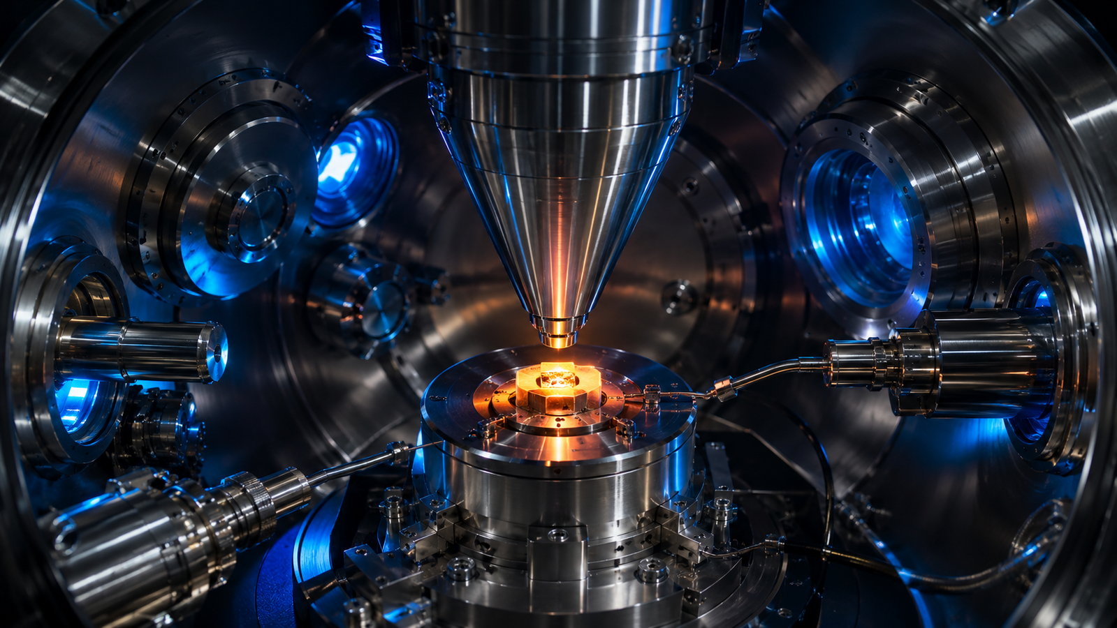
You can heat a sample in a furnace and image it afterwards — a before-and-after story with the interesting part missing. Or you can put the furnace inside the microscope and watch the change as it happens: a sintering neck growing between two particles, a grain boundary sweeping across a field of view, an oxide film cracking open. That is what an in-situ SEM heating stage does. This guide covers the physics that makes it harder than it sounds — the vacuum, the glowing sample, the drift, the gap between set temperature and true temperature — and the remarkable range of processes you can watch once those problems are handled.
1. Why watch it happen in the SEM
Post-mortem microscopy gives you snapshots: heat, quench, polish, image, repeat at the next temperature. Between snapshots, everything interesting is inferred rather than observed — and quenching itself can rewrite the story, because reversible transformations relax, surfaces reconstruct, and metastable states vanish on cooling. In-situ heating greatly reduces that inference: the same field of view, the same grains, the same particles are followed continuously through the temperature program, so a rate, an onset temperature, or a growth sequence can be measured directly on identified features instead of being reconstructed statistically from different samples.
The SEM occupies a specific niche among in-situ methods. In-situ X-ray diffraction — covered in our companion guide, In-Situ XRD: Watching Crystal Structure Evolve — reports the average crystal structure of the illuminated volume: lattice parameters, phase fractions, strain. The SEM reports local morphology: this grain boundary, this pore, this neck. The two are complements, not rivals. Systematic comparisons of high-temperature microscopy methods — for example between high-temperature SEM and confocal laser scanning microscopy on copper and tungsten alloys — show the trade-offs explicitly: electron imaging buys spatial resolution and depth of field at the cost of a vacuum environment and more demanding detection1. When the question is “what does an individual microstructural feature do as temperature rises,” the SEM heating stage is the tool built for the answer.
2. The vacuum is part of the experiment
Everything unusual about heating inside an SEM traces back to one fact: the chamber is a vacuum, typically in the 10−3–10−4 Pa range in conventional high-vacuum operation. In vacuum there is no convection. On a benchtop hotplate, moving air carries heat away and evens out gradients; in the SEM, heat leaves the sample only by conduction through whatever it touches and by radiation. That single constraint shapes the entire design of a heating stage — how it is insulated, how much power it needs, how steep the temperature gradients across a sample can be, and why the true sample temperature is a harder question than it looks (Section 7).
The vacuum also imposes discipline on the sample itself. Anything that outgasses — adhesives, solvents, porous or hydrated materials — degrades the chamber vacuum and can contaminate the column. Materials with significant vapor pressure at the target temperature will evaporate and coat nearby surfaces, including detectors and pole pieces. And some chemistry simply cannot happen: oxidation studies need oxygen. This is where environmental and low-vacuum SEM modes earn their place, admitting a controlled gas — commonly from tens to hundreds of pascals — around the sample so that reactions with a gas phase can be watched rather than suppressed. Several of the landmark studies in Section 6 were done exactly this way. The choice of vacuum mode is not a background setting; it is part of the experimental design.
3. Bulk Furnace vs MEMS SEM Heating Stages
SEM heating stages come in two broad families, distinguished by how much material they heat.
Bulk furnace stages are miniature resistive furnaces that accept millimetre-scale samples — pellets, fragments, foils. A heating element surrounds or underlies a small crucible or platform; radiation shields and a water-cooled body protect the microscope from the heat load. Carefully engineered versions reach remarkable temperatures: modifications to a commercial hot stage and its SEM allowed continuous imaging of ceramic surfaces at temperatures as high as 1450 °C, watching glass crystallization and pore evolution during sintering in real time2. Bulk stages preserve realistic sample geometry — you study the actual pellet, not a proxy — but their thermal mass makes heating and cooling comparatively slow and their power demand substantial.
MEMS micro-hotplate stages take the opposite approach: shrink the furnace to a chip. A thin suspended membrane carries a micro-patterned heater; the sample — a powder grain, a flake, a thin lamella — sits directly on the heated zone, which may be only tens to hundreds of micrometres across. Because the heated mass is microscopic, ramp rates can be extreme and power consumption tiny; refractory-metal designs such as molybdenum micro-hotplates extend chip heating to the high-temperature regime3. The trade-off is sample format: MEMS stages want small, flat, well-contacted specimens, and a millimetre pellet simply does not fit. Choosing between the families is mostly choosing between realistic bulk geometry and speed-plus-stability at the micro scale.
4. High-Temperature SEM Imaging & Detector Choice
As temperature rises, thermal radiation and thermionically emitted electrons increasingly contaminate the detected signal; above roughly 800–900 °C the problem can become severe, depending on sample emissivity, detector design, and geometry — and the detector suffers long before your eye would notice anything. The workhorse SEM detector — the Everhart–Thornley design — collects secondary electrons by accelerating them onto a scintillator whose light is piped to a photomultiplier4. A photomultiplier is exactly the wrong instrument to point at a furnace: thermal radiation from the hot sample floods the scintillator–light-pipe path with photons, and thermally emitted electrons add a further spurious signal. Meanwhile the secondary electrons that carry the image are low-energy — most below ~50 eV, escaping from only nanometres beneath the surface — which is precisely why they produce such fine surface detail, and also why they are easily swamped5. The practical result is familiar to anyone who has tried it: contrast washes out and the image drowns in glow as temperature climbs.
The remedies attack the physics directly. Backscattered electrons are far more energetic than secondaries, so a suitably shielded or heat-resistant BSE detector separates the electron signal from thermal background much more effectively than a conventional secondary-electron chain; scintillator-based BSE detectors engineered to tolerate heat have demonstrated clean imaging with heating stages up to 1050 °C in both high- and low-vacuum modes, following grain growth, recrystallization, and oxidation live6. Dedicated high-temperature imaging systems combine such detection strategies with optimized geometry and acquisition to push usable imaging further into the glowing regime7. Filtering out thermal photons, shielding the detector’s line of sight to the hottest zones, and keeping dwell times short all help. The theme is consistent: at high temperature, you stop asking the detector to ignore the furnace and start designing so it never sees it.
5. Thermal Drift and Image Registration in In-Situ SEM
Heat anything and it expands. The stage body, the sample holder, and the sample itself all lengthen as temperature rises, and at SEM magnifications even micrometres of expansion translate into the field of view sliding steadily across the screen. Drift is worst while temperature is changing — every ramp launches a new transient — and decays as the assembly approaches thermal equilibrium, which can take many minutes after each setpoint change. Working with drift is a craft: hold at temperature and let the stage settle before critical acquisitions, track features at moderate magnification instead of maximum, re-centre between frames, and keep individual exposures short so each frame is sharp even if the sequence wanders.
What cannot be prevented can be corrected afterwards. Time-lapse series are routinely re-registered in post-processing, aligning each frame to a common reference so that measurements — neck widths, grain diameters, crack lengths — are made on a stabilized sequence. Open image-analysis platforms such as ImageJ, the field’s long-standing common denominator for exactly this kind of quantitative frame-by-frame work, make alignment and measurement part of the standard workflow8. The long high-temperature observation campaigns in the next section would be unreadable without this combination of patience during acquisition and registration after it.
6. What you can watch
This is the payoff. Once vacuum, detection, and drift are under control, the SEM heating stage becomes a window onto processes that textbooks could previously only diagram.
Sintering and grain growth. The classic demonstration is ceramic sintering watched grain by grain. In-situ observation of CeO2 inside a heated environmental SEM tracked grain growth and pore elimination continuously at 1000–1300 °C, resolving 2–10 nm detail over runs lasting eight hours — individual grains could be watched growing, shrinking, and vanishing, and growth kinetics extracted from the very grains being imaged9. That is a direct, feature-level test of theory that was built decades earlier from indirect evidence: Herring’s scaling laws relating sintering time to particle size10, the Kingery–Berg analysis of initial-stage neck growth between spheres by viscous flow, evaporation–condensation, and diffusion11, Coble’s models for intermediate- and final-stage densification12, and Greenwood’s theory of coarsening, in which large particles grow at the expense of small ones13. The simulator below puts that framework on screen.
Interactive: watch a sintering neck grow
Two particles touch, and a neck forms and widens between them — the elementary event of sintering. The simulator implements the initial-stage power law of Kingery–Berg form, (x/r)n = C·t, where x is the neck radius, r the particle radius, and the exponent n depends on which transport mechanism operates; the rate constant C rises with temperature following an Arrhenius law, and Herring’s scaling makes smaller particles sinter disproportionately faster. Drag the temperature and watch the kinetics respond.
Grains, orientations, and phases. Pairing a heating stage with electron backscatter diffraction extends live observation from morphology to crystallography: high-temperature EBSD and SEM imaging have been used to follow dynamic processes — recrystallization, grain rotation, phase transformation — with orientation maps acquired as the microstructure evolves14.
Thin films letting go. A continuous thin film is usually metastable: heat it and it agglomerates into islands by solid-state dewetting, driven by surface-energy minimization through surface diffusion well below the melting point15. Watching holes nucleate, rims retract, and islands pinch off is a heating-stage staple in thin-film and catalysis research.
Surfaces changing chemistry. In solid oxide fuel cell cathodes, strontium segregates to the surface during operation and degrades performance. Heated environmental-SEM observation of La0.6Sr0.4Co0.2Fe0.8O3−δ from room temperature to 1000 °C compared oxygen, water, and air atmospheres directly, revealing where Sr-rich particles nucleate and how the atmosphere changes the kinetics16.
Oxidation and reaction fronts. In-situ heated-ESEM oxidation of uranium carbide at 723–848 K under 10–100 Pa of oxygen captured the full morphological sequence — induction, expansion, crack formation and propagation — as the carbide converted to oxide17. In steelmaking research, the same approach revealed the kinetics of non-metallic inclusion reactions directly at temperature18.
7. How hot is the sample, really?
The temperature on the controller is what the stage sensor or calibrated heater reports — a thermocouple in the furnace body of a bulk stage, an integrated sensor or a resistance-based heater calibration on a MEMS chip — not automatically the temperature of the specimen itself. In vacuum, with no convection to equalize things, the difference can be substantial: heat reaches the sample through imperfect mechanical contacts and by radiation, both of which depend on sample size, shape, surface finish, and thermal conductivity. A systematic study of sample thermal response in a 1300 °C-class SEM microfurnace showed in detail how the common assumption that furnace temperature equals sample temperature breaks down, and how the gap depends on the sample and its mounting20.
Good practice follows directly. Maximize thermal contact and keep samples small and thin so gradients across them stay modest. Allow generous soak time at each setpoint before trusting a reading. Calibrate against physics rather than electronics: observing a known transformation — the melting of a standard metal particle placed beside the sample, or a well-characterized phase transition — anchors the true local temperature at the sample position. And report honestly: a nominal furnace temperature and a calibrated sample temperature are different quantities, and papers that distinguish them age better than papers that do not.
8. How to Choose an In-Situ SEM Heating Stage
Five questions before choosing an in-situ SEM heating stage
The last point deserves emphasis: the electron beam is not a passive observer. Beam-induced heating, radiolysis, charging, and contamination depend not only on total dose but also on dose rate, beam energy, probe current, thermal contact, and chamber cleanliness — and a long in-situ campaign accumulates a great deal of everything; dose budgeting is as much part of experimental design in the SEM as it is in the TEM21. Plan magnification, dwell time, and frame rate so the beam documents the process without becoming part of it.
On the hardware side, the InSitu Pro™ heating and cooling stage family spans sixty-odd temperature-controlled platforms — optical windows, electrical probes, tensile frames, XRD domes, and dedicated SEM modules — from −190 °C up to 1700 °C, built around the same discipline this guide describes: matching stage, atmosphere, and instrument to the question. For SEM and FIB integration specifically, configuration is matched to chamber clearance, working distance, detectors, feedthroughs, and the vacuum or gas mode your experiment needs. For a structured way to narrow the options, the InSitu Pro™ Stage Selection Guide walks through the decision step by step, and the interactive Stage Selector filters the whole range by application, temperature, cooling method, and probes. If your application calls for electron-microscope integration, contact our team to discuss configuration against your chamber and detectors.
Knowledge hub
- In-Situ Heating, Cooling & Electrical Stages: A Theory Guide — the pillar overview of the whole in-situ stage family and the physics behind it.
- In-Situ XRD: Watching Crystal Structure Evolve — the companion guide to following average crystal structure while the SEM follows local morphology.
- Non-Ambient XRD Attachments: Heating, Cooling & Vacuum — how the same stage-design trade-offs play out on a diffractometer.
- InSitu Pro™ Heating & Cooling Stages — the full temperature-stage platform from −190 °C to 1700 °C.
- InSitu Pro™ Stage Selector — interactively filter the range by application, temperature, cooling method, chamber, and probes.
FAQ
What does an in-situ SEM heating stage do?
It replaces the standard SEM sample holder with a vacuum-compatible miniature furnace or chip heater, so the electron beam can image a sample continuously while a temperature program runs. Instead of comparing before-and-after images, you watch sintering, grain growth, dewetting, oxidation, or phase transformations unfold on the specific features in your field of view.
Should I choose a MEMS micro-hotplate or a bulk furnace stage?
Match the stage to the sample. Millimetre-scale pellets, fragments, and realistic bulk geometry call for a furnace-type stage; the cost is thermal mass, so ramps are slower and power demand higher. Micro-flakes, powder grains, and thin lamellae suit MEMS micro-hotplates, which heat almost nothing but the sample and therefore ramp extremely fast with excellent stability — but cannot accept bulk specimens.
Why do my images get worse as the temperature rises?
A glowing sample floods the standard secondary-electron detector — a scintillator–photomultiplier chain that is sensitive to thermal photons as well as electrons — and thermally emitted electrons add further background. Switching to backscattered-electron detection with a heat-tolerant detector, shielding the detector’s view of the hottest zones, and shortening dwell times restore usable contrast well into the visibly glowing regime.
Is the displayed temperature the true sample temperature?
Not exactly. The thermocouple sits in the furnace body, and in vacuum the sample couples to it only through imperfect contact and radiation, so the sample can lag the reading by a margin that depends on its size, mounting, and conductivity. Calibrate with a known melting point or phase transition at the sample position, allow soak time at each setpoint, and report nominal and calibrated temperatures as distinct numbers.
Can I heat in a gas atmosphere instead of high vacuum?
Yes — environmental and low-vacuum SEM modes admit a controlled gas, commonly tens to hundreds of pascals, around the heated sample. That is how oxidation, water-vapor effects, and other gas–solid reactions are studied in situ; several of the studies cited in this guide were performed in exactly this mode.
References
This article is provided by ACS Material LLC for educational purposes and describes in-situ SEM heating stages — furnace-type and MEMS micro-hotplate designs operated inside scanning electron microscopes. Temperature ranges, pressures, resolutions, and performance figures cited refer to representative designs and the specific studies referenced; the actual range, stability, imaging performance, and compatibility of a given stage depend on the model, options, sample, detectors, and microscope. Sample temperature can differ from the controller setpoint and should be validated against a certified standard under the actual experimental conditions. The interactive simulator on this page is a schematic teaching tool built on idealized models, not a substitute for measurement. For product-specific specifications, always consult the relevant technical data sheets and safety data sheets, or contact our team to confirm fit against your instrument and experiment.