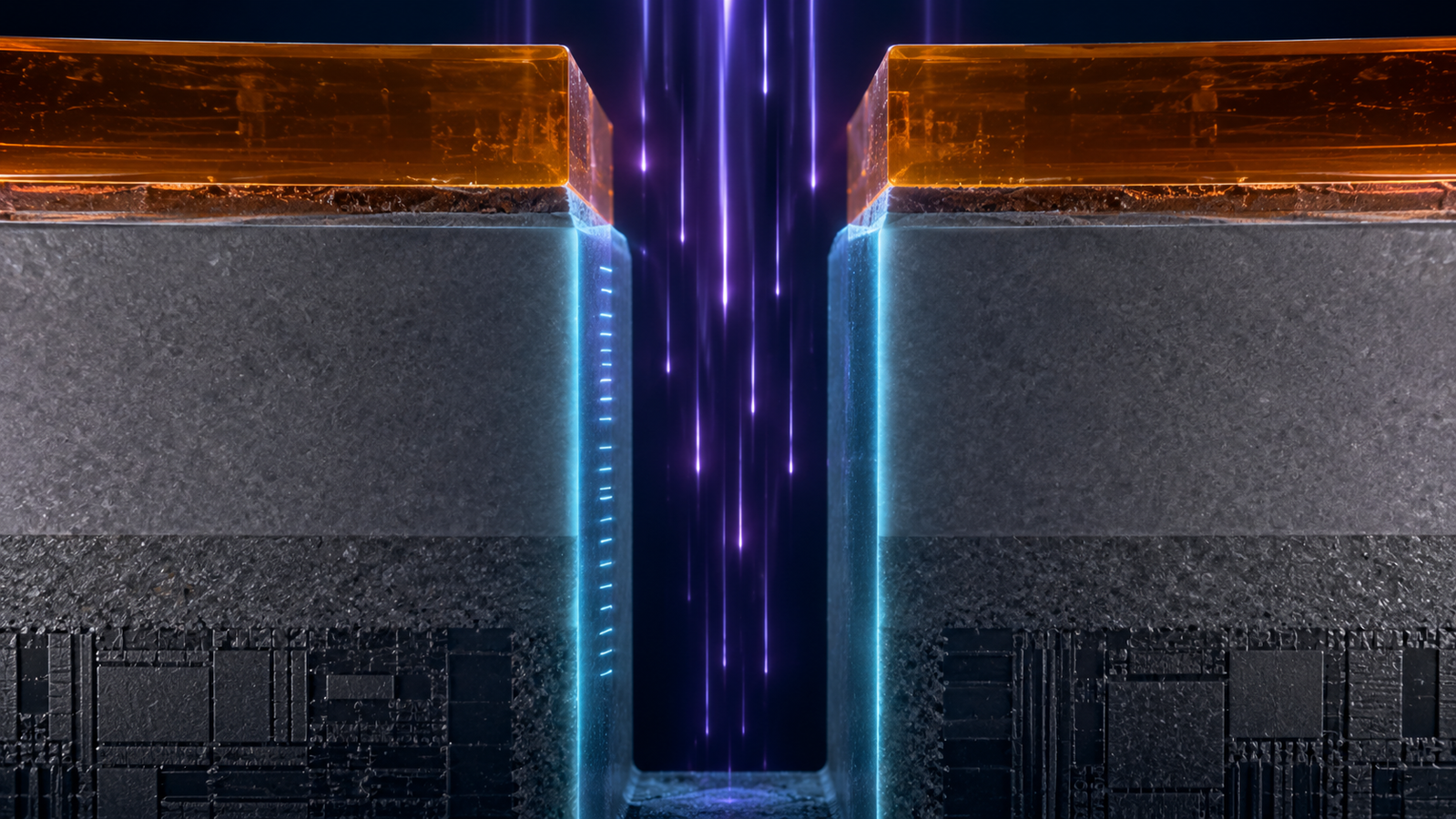
Every chip, MEMS device, and photonic circuit is a sculpture, and plasma etching is the chisel: it removes material through a mask to carve patterns measured in nanometers. Its dominance rests on a single geometric fact — a plasma can be made to etch straight down in nearly any material and pattern, without leaning on the crystal-orientation rate tricks that anisotropic wet etches depend on. But the way it earns that fact is the interesting part: pure chemistry etches fast and selectively in every direction at once; pure ion bombardment etches vertically but slowly and indiscriminately; and only their combination — the Coburn–Winters synergy behind reactive ion etching — delivers speed, selectivity, and vertical walls together. This guide walks the three mechanisms, the profiles they carve, the uniformity and damage battles that follow, and the atomic-layer frontier where etching now removes one layer at a time.
In one paragraph: plasma etching removes material through a mask by three mechanisms with opposite personalities. Reactive neutrals etch chemically — fast and selective, because only volatile products leave — but isotropically, undercutting the mask. Sheath-accelerated ions sputter — highly directional, but slow and unselective. Together they multiply: ion damage activates the floor so chemistry consumes it far faster than the ion-free sidewalls, which passivation films additionally protect — reactive ion etching, fast and anisotropic and selective. The remaining battles are uniformity (aspect-ratio and loading effects), ion damage and heating, and the atomic limit, where atomic layer etching alternates self-limited adsorb/bombard steps for sub-nanometer, near-atomic control. Production etching lives in dedicated RF tools; the physics underneath it — and the gentle organics-removal end — is benchtop territory.
1. Patterning is a subtraction problem
Every microfabricated object — transistor, MEMS mirror, microfluidic channel, photonic waveguide — is mostly defined by what was removed. A mask protects the pattern; everything unprotected must go, cleanly, to a controlled depth, without harming what stays. Wet chemistry did this first and hit a wall: most liquid etches attack in all directions at once, so features blur sideways as they deepen; the anisotropic exceptions — KOH and TMAH on silicon — lean on crystal-orientation rate differences and work only where the crystallography cooperates. Either way, the beaker ran out of road once dimensions shrank below the etch depth. Plasma etching replaced the beaker with a discharge, and the reason it conquered manufacturing is not raw speed but shape: a plasma can be persuaded to etch straight down.1 How it does that — and why neither chemistry nor physics manages it alone — is this guide's story.2
2. The etch profile lab
The simulator below etches one masked substrate three ways. Pure chemical: neutral radicals arrive from every direction, and the cavity bulges sideways under the mask — the isotropic undercut that killed wet etching's scaling. Pure sputter: sheath-directed ions carve vertical walls, but slowly, and the mask erodes with everything else. Ion + chemistry: the combination etches fast and vertical, with a passivation film protecting the sidewalls. Watch the profiles — the shapes are the entire argument.
3. Predominantly chemical: fast, selective, shapeless
The chemical route generates reactive neutrals in the discharge — fluorine atoms from CF₄ or SF₆, oxygen atoms for organics — which react with the surface to form volatile products that simply pump away — gas-phase plasma chemistry doing the reagent manufacturing.2,3 Volatility is the secret handshake: silicon plus fluorine makes gaseous SiF₄, so silicon etches; the mask and untargeted layers make no volatile product, so they survive. That gives chemical etching its two virtues, speed and selectivity, and its fatal vice: radicals are gas molecules, arriving from every direction and reacting wherever they land, so the etch is isotropic — it undercuts the mask by roughly the etched depth. Perfect for stripping photoresist, cleaning residues, and texturing polymers — the family that also serves low-pressure cleaning systems and biomaterial surface work — and unusable, alone, for a vertical nanometer-scale line.4,5,6
4. Predominantly physical: direction without discretion
The physical route uses the sheath — the thin field region every plasma wraps around a surface — as an ion gun. Ions fall through it essentially perpendicular to the wafer and arrive as momentum: each impact chips atoms loose ballistically.7,8 Direction is superb; everything else is expensive. Sputter yields are low, so the etch crawls; and momentum has no chemistry, so it is unselective — the mask erodes along with the target, and sputtered atoms can redeposit where they are not wanted. Pure sputter etching proved vertical profiles were possible; it also proved that direction without selectivity cannot pay for itself.2
5. Ion-assisted chemistry: the RIE synergy
The field's founding experiment put the two together and found something better than their sum. Coburn and Winters showed that a surface exposed to reactive gas and ion bombardment simultaneously etches far faster than either exposure alone — the ions damage and activate the surface so the chemistry consumes it at multiplied rates.9 Because ions arrive only vertically, the multiplication happens only on the floor of the feature; sidewalls, untouched by ions, etch at the slow chemical baseline — and in modern recipes barely at all, because deliberately deposited sidewall passivation films shield them while ion bombardment keeps the floor swept clean.1 The result is reactive ion etching: fast where ions land, protected where they do not, selective because the chemistry still chooses its products. Anisotropy becomes a tunable, with pulsed-plasma operation offering finer control over the charge and radical balance.10 This synergy, iterated for forty years, is the subtraction machine underneath every chip.11
| Mechanism | Rate | Selectivity | Directionality | Mask cost |
|---|---|---|---|---|
| Predominantly chemical | High | High — set by volatile-product chemistry | Low — tends isotropic | Undercut beneath the mask |
| Predominantly physical (sputter) | Low | Low — everything sputters | High — sheath-directed | Mask erodes and facets |
| Ion-assisted (RIE) | High — synergy multiplies | High — chemistry-set | High — ion-set, passivation-guarded | Managed by chemistry and passivation |
6. Uniformity, damage, and the atomic limit
Winning the profile war exposed subtler battles. Uniformity: etch rates depend on feature geometry and pattern density — aspect-ratio-dependent etching and microloading — so identical recipes etch different layouts differently, a problem Gottscho and colleagues framed for the field.12 Damage and heat: the ion bombardment that grants anisotropy also implants, roughens, and warms — gas and surface temperature are process variables, not bystanders.13,14 And at the leading edge, features a few atoms wide demand removal a few atoms at a time: atomic layer etching splits the Coburn–Winters synergy into alternating self-limited steps — adsorb, then bombard — trading raw rate for near-atomic, sub-nanometer control — per-cycle removal need not equal exactly one monolayer, and thermal as well as plasma-assisted variants exist.15 Roadmaps for plasma science put exactly this frontier — atomically precise, damage-controlled etching — near the center of the field's next decade.16,17 It matters beyond silicon: the same precision tools now pattern and thin 2D materials, where a monolayer is the entire device.18,19
7. Etch-gas safety, exhaust & abatement
The chemistry that makes plasma etching work makes its plumbing serious. Fluorinated and chlorinated feed gases are toxic, corrosive, or both; unreacted feed and reaction by-products leave with the pump exhaust and must be scrubbed or otherwise abated before the vent — treatment is part of the process design, not an accessory. Several fluorinated etch gases are also potent, long-lived greenhouse gases, and the semiconductor industry runs formal measurement and abatement programs around their use and emission.1 The practical reading for a laboratory: reactive-gas etching belongs on tools engineered for it, with gas cabinets, monitored delivery, and treated exhaust — while the benign end of the spectrum (oxygen and argon chemistry on benchtop platforms) is where hands-on learning safely lives.
8. Where the hardware lives
Production etching is the domain of dedicated RF tools — capacitive and inductive reactors with biased chucks, engineered gas chemistries, and endpoint metrology — usually purchased, not assembled.20,21 Two honest adjacencies remain for a materials lab. First, the physics is learnable at benchtop scale: a CTP-2000K plasma supply sustains both atmospheric and reduced-pressure glow regimes in which sheaths, ion bombardment, and plasma–surface chemistry can be studied directly, and a DBD experiment cell covers the atmospheric side of plasma–surface work — a teaching and surface-chemistry platform, not a production RIE tool. Second, the gentle end of etching is genuinely accessible: oxygen-plasma removal of organics — resist stripping's cousin, descumming, polymer texturing — runs happily on laboratory discharges — industrially, microwave downstream sources built this stripping niche22 — and atmospheric-pressure discharges extend it into open air, where jets have demonstrated localized polymer etching.23,24,25 Know which side of that line your problem sits on, and the purchasing decision writes itself.
Knowledge hub
- Plasma Processing Guide — the pillar overview of cold plasma, discharges, and power supplies.
- Plasma Cleaning — the gentle end of material removal — contamination instead of pattern.
- Electron vs Gas Temperature — the cold-plasma asymmetry that makes selective surface chemistry possible.
- Impedance Matching — how etch tools deliver and meter the RF power behind the sheath.
- CTP-2000K Plasma Power Supply — the DBD, glow, and arc platform where sheath and surface physics are studied.
- DBD Experiment Device — the benchtop cell for atmospheric plasma–surface work.
FAQ
What is the difference between plasma etching and RIE?
Usage blurs, but the useful distinction is mechanism: "plasma etching" covers all discharge-driven removal, while reactive ion etching names the synergistic mode — reactive chemistry plus directional ion bombardment on a biased substrate — that delivers anisotropic profiles. Most patterning work people call plasma etching is RIE-family.
Why does my etch undercut the mask?
Because the chemical component is winning. Isotropic radical etching proceeds sideways beneath the mask edge at rates comparable to downward; if undercut is growing, the recipe lacks ion assistance or sidewall passivation — more directional bias, passivating chemistry, or lower pressure are the standard levers.
What does selectivity mean in etching?
The rate ratio between the material you want removed and the materials you need kept — mask and underlayer. Chemical pathways supply it, because volatility is material-specific; pure sputtering has almost none. Real recipes are negotiated compromises between selectivity, rate, and profile.
What is atomic layer etching (ALE)?
The self-limited version of the RIE synergy: one step adsorbs a reactive layer that saturates and stops; a separate step supplies just enough ion energy to remove the modified layer — close to, though not always exactly, one monolayer per cycle; repeat. Rate is sacrificed for sub-nanometer control.
Can plasma etch polymers and organics?
Readily — oxygen-based plasmas convert organics to volatile CO, CO₂, and H₂O, which is exactly how photoresist stripping and descum work, and how gentle laboratory discharges texture and clean polymer surfaces. The recipe question is protecting whatever must remain.
Do I need a cleanroom etcher to study plasma etching?
To fabricate devices, yes. To study the physics that makes etchers work — sheaths, ion energetics, plasma–surface chemistry, dose control — a benchtop low-pressure glow platform is the honest and affordable classroom, and it transfers: the parameters you learn to read there are the ones the production tool recipe screen is quietly encoding.