
A voltmeter and a current source give you resistance. They do not give you resistivity, sheet resistance, carrier density or mobility — the quantities a materials paper actually reports. The bridge between the terminal reading and the material parameter is built from two things: geometry, which turns V/I into ρ or Rs through probe arrangements and correction factors, and a magnetic field, which splits the conductivity into how many carriers and how fast they move. This article is the geometry-and-field chapter of the electrical cluster: collinear four-point probes, van der Pauw, Hall bars, field-reversal protocols, and what the temperature axis adds when all of it runs on a variable-temperature stage. The hardware and transport overview and the R(T) fitting methodology are its two companions; here we take the measured numbers and turn them into material parameters.
1. Why Four Probes — and Why That Is Only the Start
Two-terminal measurement adds everything in the current path — lead wires, contact interfaces, spreading resistance — to the number on the meter, and at temperature extremes the contact contribution can drift, rectify or dominate outright. Four-terminal sensing routes the current through one pair of contacts and reads the voltage across another pair that carries essentially none, so those series terms drop out of the reading; the physics, the contact behaviour and the pitfalls are treated in the companion overview of variable-temperature probe stages. What four probes do not do is tell you what the surviving number means. V/I is a resistance; converting it into a material property is a geometry problem, and geometry is what the rest of this article is about — a problem catalogued in detail, correction factor by correction factor, in the technique’s hundred-year retrospective1.
2. The Collinear Four-Point Probe
The oldest arrangement — four equally spaced contacts in a line, current through the outer pair, voltage across the inner pair — goes back a century to Wenner’s earth-resistivity work and entered semiconductor practice through Valdes’s germanium measurements2. On a sample that looks semi-infinite compared with the probe spacing s, the geometry integrates out to a clean closed form: ρ = 2πs·(V/I). Every departure from “semi-infinite” — finite thickness, nearby edges, small lateral size — multiplies that formula by a correction factor, and the classic factor tables for thin rectangular and circular samples were worked out by Smits3.
The limit that matters most in film work is the thin-sheet limit, where the sample thickness t is much smaller than s. There the measurement stops caring about t altogether and delivers the sheet resistance directly: Rs = (π/ln 2)·(V/I) ≈ 4.532·(V/I), with bulk resistivity recovered as ρ = Rst when — and only when — the thickness is known and uniform3. Two practical cautions travel with the collinear array. First, the probe spacing enters the bulk formula linearly, so a spacing error is transferred one-for-one into ρ. Second, the correction factors assume the probes sit far from edges in units of s; near an edge or on a small sample the factor moves, and the retrospective review tabulates how far one can push before the percent-level errors begin1.
3. Van der Pauw Method: Equation, Assumptions & Corrections
In 1958 L. J. van der Pauw published a result that still feels like a magic trick: for a flat sample of arbitrary shape, four small contacts on the perimeter suffice to determine the sheet resistance — no lateral dimensions measured at all4. (Bulk resistivity, ρ = Rst, still requires an accurate thickness.) Two configurations are recorded: drive current through one adjacent contact pair and read voltage across the opposite pair (R1), then rotate all roles by one contact (R2). The two resistances are locked to the sheet resistance through the van der Pauw equation, exp(−πR1/Rs) + exp(−πR2/Rs) = 1, solved numerically in general and collapsing, for a symmetric sample where R1 = R2 = R, to Rs = πR/ln 2 ≈ 4.532R — the same ln 2 constant as the collinear thin-sheet limit, arriving from a very different direction5.
The theorem’s price is its assumptions, and they are strict: a homogeneous, electrically isotropic plate of uniform thickness; a singly connected sample (no holes); contacts that are small compared with the sample; and contacts placed on the perimeter, not inset. Violate them and the exactness quietly leaves — finite contact size and inset placement produce systematic errors that have been mapped in detail, growing with the contact’s fractional size and its distance from the edge15. Two working habits catch most trouble. Measure both configurations always — the full van der Pauw equation requires both. Read the ratio with care: for an arbitrary shape, a large R1/R2 can arise purely from geometry and contact placement even in a perfectly homogeneous, isotropic sample — that is exactly the case the exponential equation was built to handle. Only when the sample and contact layout were designed symmetric does an unexpectedly large ratio become a useful prompt to check contact size, inset contacts, inhomogeneity, anisotropy or a violated assumption. And re-verify the contacts at each temperature extreme, because a contact that has drifted rectifying breaks the linearity the theorem silently assumes. The reward for the discipline is substantial: the same four perimeter contacts, with a field applied, measure the Hall effect on the identical sample — which is why van der Pauw remains the default geometry for combined resistivity-plus-Hall work.
4. The Hall Bar: Geometry Made Explicit
The Hall bar takes the opposite philosophy from van der Pauw: instead of tolerating arbitrary shape and correcting for it, make the geometry explicit — which often reduces correction uncertainty, though it does not eliminate geometric error. A rectangular channel of known width w and thickness t carries the current; voltage taps along one edge, separated by a known length L, read the longitudinal voltage for resistivity (ρ = (Vxx/I)·wt/L); a pair of taps facing each other across the channel reads the transverse Hall voltage. Longitudinal and transverse signals come out of separate, dedicated contact pairs — which is precisely the point.
The trade is fabrication for clarity. A Hall bar must be patterned, cut or masked into shape, and its parameters enter the analysis directly, so w, t and L must actually be known — the geometry does not forgive the way van der Pauw does. In exchange, the current path is deliberately constrained and can be made approximately uniform in the central measurement region: the aspect ratio can be chosen long enough (L/w of several) that the voltage taps sit away from the current contacts, and opposite Hall taps can be placed with minimal misalignment. Finite contact size, current crowding near the injection contacts, a too-short channel or too-wide voltage arms, and errors in w or t can still bias both the longitudinal and the Hall reading — smaller sins than an uncorrected arbitrary shape, but not zero. For low-signal work — low mobility, thin samples, small Hall voltages — that explicitness is usually worth the fabrication effort, and it is the geometry in which the Hall effect’s cleanest chapters, up to and including its quantized extreme, were written6.
The three geometries, side by side:
| Method | Best suited for | Required geometry | Main output | Main caution |
|---|---|---|---|---|
| Collinear four-point | Large films, wafers, quick mapping | Known probe spacing + correction factors | Rs or ρ | Edge, thickness and spacing corrections |
| Van der Pauw | Irregular thin samples; combined ρ+Hall | Homogeneous isotropic plate, small perimeter contacts, no holes | Rs plus Hall on the same contacts | Contact size and placement; thickness for ρ |
| Hall bar | Patterned devices; low Hall voltages | Known w, t, L and tap layout | ρxx, RH, μH | Fabrication effort; current crowding; finite contacts |
5. Hall Effect vs Temperature: Carrier Density & Mobility
Edwin Hall’s 1879 experiment answered a question Maxwell had waved away: the magnetic force acts on the current in the conductor, deflecting the moving carriers sideways until a transverse electric field builds up to balance it7. That balance is the measurement — but the honest order of operations starts one step earlier. First extract the odd-in-field transverse slope and define the Hall coefficient, RH = (t/I)·dVxy,odd/dB. Only then, under a single-dominant-carrier model, invert it: the Hall density is nH = 1/|qRH| (for a two-dimensional sheet, ns = I/(|q|·dVH/dB), the thickness dropping out), and combining with the zero-field resistivity gives the Hall mobility μH = |RH|/ρ. These are Hall quantities: they equal the true carrier density and drift mobility only when the single-carrier and Hall-factor assumptions actually hold.
Two bonuses ride along, each with its condition. The sign of RH identifies the dominant carrier polarity — electrons and holes deflect to opposite sides — provided the current direction, field direction and voltage-lead polarity are documented and the normal Hall term dominates; an undocumented lead swap flips the apparent carrier type. And the Hall factor deserves more than an asterisk: writing RH = rH/(qn) makes the relations explicit — the simple Hall density is nH = n/rH and the Hall mobility is μH = rHμdrift, where rH depends on band structure, anisotropy, degeneracy, scattering mechanism, strain and temperature and is not universally close to one8. And when several bands conduct in parallel, when the material is magnetic (anomalous Hall contributions), or when Rxy(B) is visibly nonlinear, the one-slope single-carrier inversion is simply not valid — multicarrier analysis is its own discipline. Everything else in this article — geometry discipline, contact verification, reversal protocols — exists to make sure the VH that enters these formulas is actually the Hall voltage and not an impostor.
6. Field and Current Reversal for Hall Measurements
The transverse voltage you measure is never purely VH. However carefully a Hall bar is patterned or van der Pauw contacts are placed, the two “opposite” taps are never exactly on the same equipotential line, so a fraction of the longitudinal voltage — a misalignment offset — rides on the reading. On top of it sit slowly drifting thermoelectric voltages generated wherever dissimilar conductors meet a temperature gradient, the same Seebeck physics that thermoelectric devices harvest on purpose9. In low-mobility or thin samples the true Hall voltage can be microvolts while the impostors are tens of microvolts; without a cleanup protocol, the impostors win.
The protocol exploits symmetry. The Hall voltage is odd in B: reverse the field and it flips sign, while the misalignment offset — to leading order — does not. So the antisymmetric combination VH = [V(+B) − V(−B)]/2 removes the offset, and what the offset leaves behind (its own weak, even field dependence from magnetoresistance) is second-order. Thermoelectric drifts, by contrast, are independent of the current direction while the Hall and offset terms flip with it, so current reversal subtracts them out. The complete ritual is the four-combination antisymmetrization — Vodd,odd = [V(+I,+B) − V(+I,−B) − V(−I,+B) + V(−I,−B)]/4 — which isolates the component odd in both current and field, suppressing static thermoelectric offsets and leading longitudinal leakage at once; it is standard practice in low-level transport for exactly this reason10. The symmetry table also makes explicit what reversal cannot do: a genuine anomalous Hall contribution is odd/odd like the normal term, so it survives the ritual — separating the two is analysis, not averaging.
| Signal component | Under current reversal | Under field reversal |
|---|---|---|
| Normal Hall voltage | Odd | Odd |
| Misalignment / longitudinal leakage | Odd | Even (leading order) |
| Static thermoelectric offset | Even | Even |
| Magnetoresistance leakage | Odd | Mostly even |
| Anomalous Hall contribution | Odd | Odd — not removed by reversal |
A full field sweep adds one more layer of protection: fitting the slope of V against B uses every point, averages the noise, and makes residual even-in-B contamination visible as curvature rather than silently biasing a single-point reading — the failure mode the simulator below is built to demonstrate. One prerequisite travels with the slope method: it is meaningful only over a field range where Rxy(B) is demonstrably linear — visible curvature signals multiple carriers, anomalous contributions, a field-dependent Hall factor or other non-single-carrier physics, and calls for the multicarrier toolbox rather than a straight line.
7. What the Temperature Axis Adds
A zero-field R(T) curve measures the product n(T)·μ(T) and cannot tell the factors apart — the central entanglement noted throughout the companion methodology guide. Under an appropriate single-carrier model and Hall-factor treatment, Hall-plus-resistivity measurements at each temperature perform the separation: the Hall density nH(T) from the odd-in-field slope, the Hall mobility μH(T) from its combination with ρ(T). That separation is what turned early semiconductor curves into physics — the classic silicon study read donor and acceptor ionization directly from the freeze-out of n(T) and scattering physics from the temperature dependence of mobility, resolving what resistance alone had left ambiguous11.
Each factor tells its own story. The carrier density traces the occupation statistics — freeze-out at low temperature, the exhaustion plateau where n counts the dopants, the intrinsic climb at high temperature — so a variable-temperature Hall series is the most direct dopant-activation measurement there is. The mobility traces the scattering: phonon-limited transport falls with warming (a power law in the neighbourhood of T−3/2 in simple bands), ionized-impurity scattering strengthens with cooling (rising roughly as T3/2), and the crossover between them dates the dominant mechanism at each temperature8. Two-dimensional materials made this workflow famous all over again: the first graphene transport papers were, at their core, variable-temperature Hall-and-field-effect measurements12, and suspending the flakes to remove substrate scattering exposed the intrinsic phonon-limited mobility underneath13. And the far end of the same axis is legendary: cool a clean two-dimensional system far enough in a strong field and the Hall resistance stops obeying the classical formula altogether, locking onto quantized plateaus — the discovery that made Hall measurement a pillar of metrology6. On a −190 °C to 600 °C stage, which of the freeze-out, extrinsic/exhaustion and intrinsic regimes fall inside the window depends on the dopant ionization energy, compensation, carrier concentration, band gap and scattering law — shallow donors may freeze out mostly below 83 K, and wide-gap intrinsic conduction may sit far above 873 K. The window captures one or more regimes for a given material, not all three for every material — and for many mainstream doped semiconductors it is exactly the range where materials development happens.
8. Interactive: The Hall Field-Sweep Lab
The simulator below stages the Section 6 problem. It generates a synthetic Hall field sweep — transverse voltage versus B from −1 T to +1 T — for an n-type sample whose true carrier density you set, then contaminates the data with a misalignment offset you control and realistic voltage noise. Three read-outs extract the carrier density three ways: from a single point at +1 T (the tempting shortcut), from the field-reversal pair, and from a straight-line fit to the full sweep. Watch what happens to each as you raise the offset or push the density high enough that the true Hall voltage sinks toward the noise.
The lesson is the protocol’s value made visible. The single-point estimate swallows the offset whole — at high density, where |VH(1 T)| is tens of microvolts, a comparable offset corrupts the magnitude by a factor rather than a percentage, and can even flip the apparent carrier sign. The reversal pair cancels the constant offset at the cost of using two points; the slope fit cancels it too — the fitted intercept absorbs it — while using every field point against the noise. Neither is immune: residual random error remains in both, visibly so under the Regenerate button, and neither protects against field-calibration error or genuinely nonlinear Rxy(B). One honesty note carried over from the companion articles: the offset here is modelled as field-independent, which is the leading-order truth; real misalignment also carries a weak even-in-B magnetoresistance component and thermal drifts, which is why the full (±I, ±B) ritual — beyond what this teaching model simulates — remains the standard for publication-grade numbers.
9. The Geometry and Field Error Budget
The error budget of a four-probe or Hall campaign is dominated by terms that no voltmeter specification mentions. Geometry first. In the collinear array the spacing s enters the bulk formula linearly, so a 2% spacing uncertainty is a 2% resistivity uncertainty before anything else happens. In van der Pauw work the geometric sins are finite contact size and inset placement, with errors that have been mapped as functions of contact size over sample size1. Thickness deserves its own line: it converts Rs to ρ and sits inside the Hall density formula, so δt/t propagates one-for-one into both — for thin films, t is routinely the single largest uncertainty in the budget5.
Then the field and the sample’s own physics. The magnet needs calibrating at the sample position, and its uniformity across the sample sets a floor on how well “B” is even defined. Excitation current must clear two hurdles: large enough that VH beats the noise and offset floor, small enough that self-heating does not shift the sample temperature — the trap tightening as samples shrink14. Contacts drift with temperature and can turn rectifying at the extremes15, which corrupts the linearity every formula in this article assumes — hence contact I–V checks at both ends of the range, not just at the start. And the temperature axis itself carries the calibration, offset and lag terms of the companion methodology guide, anchored ultimately to the practical temperature scale16; a Hall density quoted at “77 K” is only as good as the evidence that the sample was at 77 K. Low-level measurement practice — guarding, settling times, reversal averaging — is the final layer, and the standard references repay reading before the first cooldown10.
10. A Measurement Protocol: From Contacts to Reported Numbers
1. Choose the geometry for the question. Uniform thin film and combined ρ-plus-Hall: van der Pauw. Low signal, low mobility, or anything needing clean simultaneous Rxx and Rxy: Hall bar. Quick comparative mapping on large samples: collinear array.
2. Verify the contacts where it hurts. Current–voltage sweeps on each contact pair at room temperature and at both temperature extremes; ohmic and stable is the entry ticket, not the conclusion.
3. Establish current linearity. Repeat a fixed measurement at two or three currents; keep the level where the answer has stopped moving and self-heating checks pass.
4. Measure the zero-field baseline properly. Both van der Pauw configurations (their ratio is your anisotropy and homogeneity alarm), or the Hall bar’s longitudinal channel, with current reversal.
5. Run the field protocol. Full sweep where time allows, symmetric ±B always, the four-combination (±I, ±B) average as the default ritual; extract VH from the odd-in-B component.
6. Add temperature last, and report everything. Step-and-hold programs per the companion methodology guide; at each setpoint, the full field protocol. The report carries the geometry and its dimensions, the correction factors applied, B, I, the temperature validation, and the rH assumption — the test, as ever, being that a stranger with your raw sweeps reaches your n and μ without asking you anything.
11. Hardware Notes: Running This on a Stage
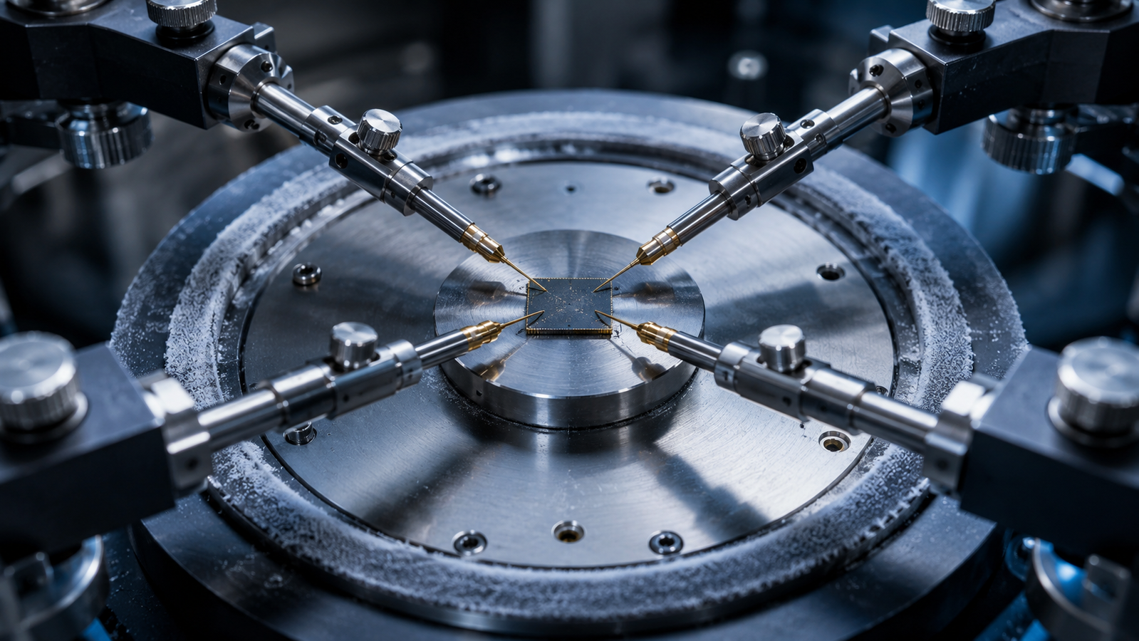
Everything above assumes four independently positionable probes on a temperature-controlled platform — and, for the Hall portions, hardware that a magnetic field can live with. The InSitu Pro™ AECH600S / AECH400SV electrical stage provides four movable magnetic-mount probe holders with BNC feedthroughs and ±0.1 °C stability across −190 °C to 600 °C (air chamber) or −190 °C to 400 °C (vacuum) — a general platform for the four-terminal portions of this article: R(T), collinear and van der Pauw contact layouts, with the usual caveat that stage stability is not sample accuracy. Hall compatibility is configuration-specific. A Hall experiment needs a calibrated magnet geometry and non-magnetic construction near the sample and probe region — which is precisely why the catalogued Hall-capable configuration, the AEH1000S-HE, is built on a non-magnetic sample stage for high-temperature work; cryogenic Hall configurations and magnet integration should be confirmed at quotation. For the broader family, see the electrical stage line or let the stage selector match the experiment to a configuration.
- Electrical Heating & Cooling Stage (AECH600S / AECH400SV) — four movable probe holders, BNC feedthroughs, ±0.1 °C: a platform for the four-terminal portions of this article (R(T), collinear, van der Pauw).
- AEH1000S-HE — the catalogued non-magnetic, Hall-capable high-temperature configuration for Hall-effect work.
- Variable-temperature electrical probe stages: the overview — hardware anatomy, contact physics and measurement pitfalls across the electrical family.
- Measuring R(T) in-situ: the fitting methodology — temperature programs, Arrhenius windows, error budgets: the data-analysis companion to this article.
- All InSitu Pro™ electrical stages — the complete electrical-application line, or use the interactive stage selector.
12. FAQ: Four-Probe and Hall Measurements
13. Keep Exploring the InSitu Pro™ Knowledge Hub
This article completes the electrical cluster of the InSitu Pro™ knowledge hub. To keep going:
- In-situ heating, cooling & electrical stages: a theory guide — the pillar article on how temperature-controlled stages work.
- In-situ electrical probe stages: variable-temperature transport — hardware, contacts, pitfalls and stage selection for the electrical family.
- Resistance vs temperature: measuring R(T) in-situ — the fitting-methodology companion: programs, windows, hopping, Tc and error budgets.
- In-situ oxidation studies by optical microscopy — the chemistry that can rewrite a sample mid-measurement.
- How to choose an in-situ heating & cooling stage — the five-step selection guide with interactive simulators.
References
This article discusses four-probe, van der Pauw and Hall measurement methodology in general terms. Formulas, correction factors, protocol steps and the regimes they assume are idealized and depend on sample geometry, homogeneity, contact quality, instrumentation and configuration; real measurements should be validated against the published literature, applicable standards, your own calibrations and the manufacturer’s datasheets before quantitative use. The interactive simulator is a schematic teaching tool — its data are synthetic, generated from a stated single-carrier model with artificial noise and a simplified field-independent offset — and is not a substitute for measured Hall data. Magnet integration on heating-and-cooling stages is experiment-specific; contact ACS Material to discuss configurations and specifications for your application.