
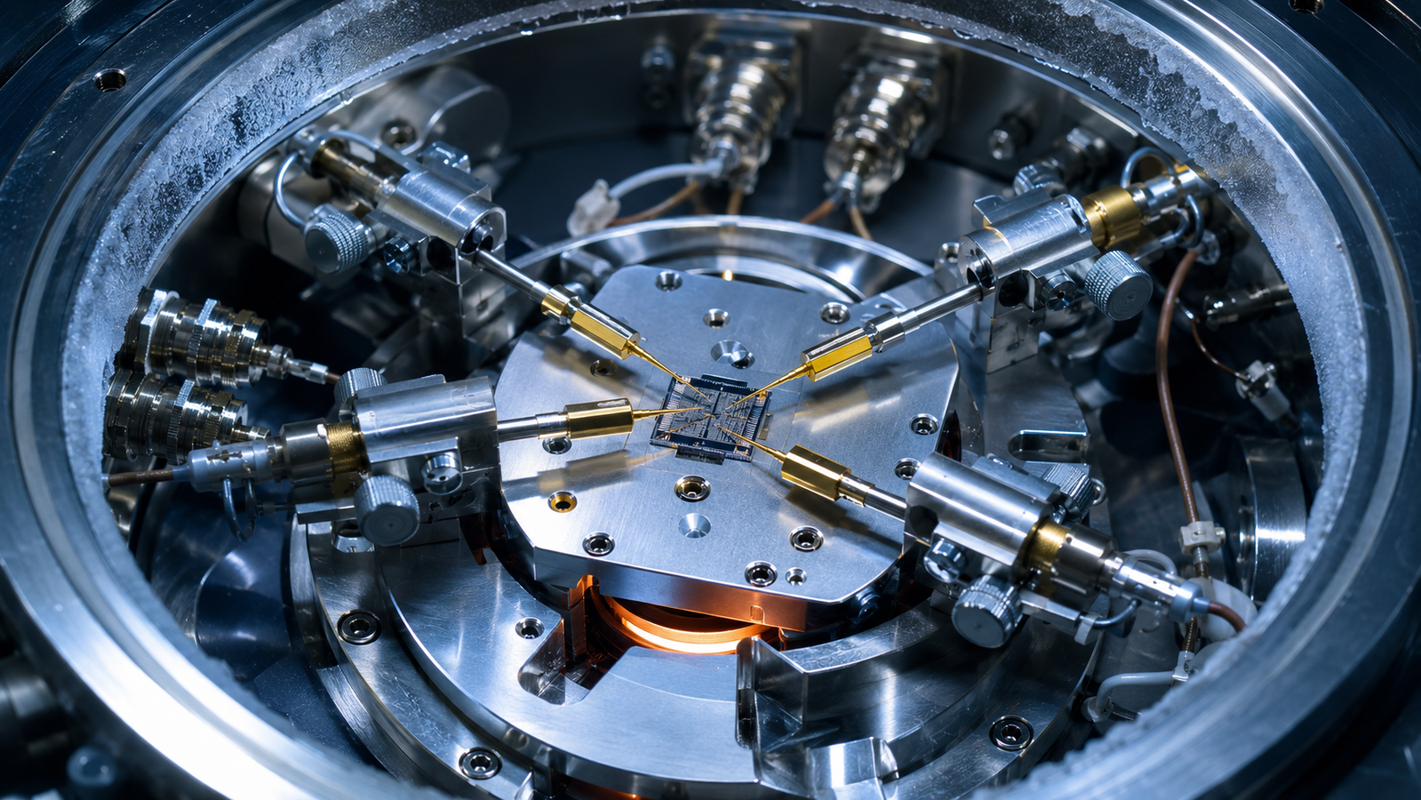
A resistance value without a temperature attached to it is half a measurement. Quote a metal film at 5 Ω, a semiconductor at 2 kΩ, an oxide at 3 MΩ — each number is true only at the temperature where it was taken, and each material will rewrite it, in its own characteristic way, the moment the thermometer moves. That temperature dependence is not a nuisance to be corrected away. It is the signature: the shape of R(T) tells you whether carriers are scattering off phonons or hopping between localized states, whether dopants are ionized or frozen out, whether a film has gone superconducting or an oxide has crossed a metal–insulator transition. An in-situ electrical probe stage is the instrument that captures this signature under a microscope — a sealed, temperature-controlled chamber from −190 °C to 600 °C with micropositioned probes touching the sample, signal lines running out to a source meter, and an optical window so you can watch the sample while you measure it. This guide covers the physics behind temperature-dependent transport, how to read an R(T) curve, why four probes beat two, what contacts do as temperature changes, the classic measurement pitfalls, and how to choose a variable-temperature probe stage for your own experiments.
1. Why Resistance Needs a Temperature Axis
The idea that a full R(T) sweep is worth far more than a single room-temperature reading is as old as semiconductor physics itself. In 1949, Pearson and Bardeen mapped the resistivity and Hall coefficient of silicon from 87 K to 900 K and used the temperature dependence — not any single value — to extract the carrier concentrations, the mobilities and the donor and acceptor ionization energies that made silicon an engineerable material1. A single point on that curve would have said almost nothing; the sweep said nearly everything.
The reason is that resistance folds together several microscopic quantities — how many carriers exist, how fast they move, and what scatters them — and each of these responds to temperature through a different physical mechanism with a different functional form. Sweep the temperature and the mechanisms separate: an exponential rise here betrays thermal activation, a power-law fall there betrays phonon scattering, a discontinuity marks a phase transition. Temperature is the axis along which transport physics becomes legible.
Practically, this is also the axis along which devices live or die. A sensor calibrated at 25 °C will be asked to work at −40 °C on a winter morning and at 125 °C inside an engine bay; a power device self-heats far above ambient; a detector may be cooled toward liquid-nitrogen temperature to quiet its noise. Measuring a material or a test structure across the whole relevant temperature window — on the same sample, in the same contact geometry, in one continuous run — is precisely what a variable-temperature probe stage is built to do.
2. Metals: Phonons, Purity and the Residual-Resistance Ratio
In a metal, the carrier density is essentially fixed — the electron sea neither grows nor shrinks appreciably with temperature — so R(T) is a pure scattering story. Near and above room temperature, the dominant scatterers are phonons, whose population grows roughly linearly with T, and so does the resistivity: copper, silver, gold, platinum all show the familiar quasi-linear rise that makes platinum such a good resistance thermometer. Cool the metal down and the phonon bath thins out dramatically. Bloch's 1930 treatment of conduction electrons scattering from lattice vibrations showed that in the low-temperature limit the phonon-limited resistivity should collapse as T⁵ — the celebrated Bloch law, later generalized into the Bloch–Grüneisen description that interpolates smoothly between the T⁵ regime and the high-temperature linear regime2.
The phonon term, however, does not fall to zero on its own terms forever. At low enough temperature every real metal levels off at a residual resistivity set by whatever temperature-independent scatterers it contains: impurity atoms, vacancies, dislocations, grain boundaries. To a good approximation the two contributions simply add — the rule of thumb known as Matthiessen's rule — so the measured curve is a temperature-dependent phonon term riding on a sample-specific constant floor.
That floor is diagnostic gold. The ratio of the room-temperature resistance to the residual low-temperature resistance — the residual-resistance ratio, RRR — is a standard one-number purity and crystalline-quality metric for metals and superconducting wires precisely because the numerator is dominated by universal phonon physics while the denominator is dominated by the defects unique to your sample; low-temperature measurement practice treats RRR as a routine acceptance test for conductor quality3. A cryo-capable probe stage reaching −190 °C (83 K) does not reach the deep-cryogenic plateau of the purest metals, but for thin films, alloys and practical conductors — whose residual term is comparatively large — the curvature and flattening of R(T) between room temperature and 83 K already reveals comparative quality trends. It does not, however, directly measure the conventional residual-resistance ratio, which is normally defined against resistance near the residual plateau — often around 4.2 K — or against a separately validated extrapolation to it.
3. Semiconductors: Activation, Exhaustion, Freeze-Out
Semiconductors invert the metallic story: here the carrier density is the strong function of temperature, and it typically overwhelms the mobility term. The canonical R(T) of a doped semiconductor, read from high temperature downward, has three acts14. At the top sits the intrinsic regime, where electron–hole pairs excited across the band gap flood the sample and resistivity plunges exponentially with an activation energy near half the gap. In the middle lies the extrinsic or exhaustion plateau, where essentially every dopant is ionized, the carrier density is pinned at the doping level, and the gentle temperature dependence that remains comes mostly from phonon-limited mobility — this is the regime in which most devices are designed to operate. At the bottom comes freeze-out: thermal energy no longer suffices to ionize the dopants, carriers re-condense onto their donor or acceptor atoms, and resistance climbs steeply again with an activation energy set by the dopant ionization level. The three-act picture is an idealized framework rather than a universal sequence: compensation, degeneracy, variable-range hopping, contact barriers and parallel conduction paths can mask or replace one or more of the acts in real samples.
Plotted as ln R against 1/T — the Arrhenius representation — each activated regime becomes a straight line whose slope is the activation energy divided by the Boltzmann constant (with a factor that depends on the regime). This is the single most-used analysis in variable-temperature transport: two decades of resistance change over an accessible temperature window turn into a band-gap or ionization-energy number with a ruler and a fit. A linear region of ln R versus 1/T yields an activation energy only within a justified conduction model, though — mobility changes, compensation and parallel channels can all tilt the slope, so the fitting range must be chosen deliberately and reported. A stage spanning −190 °C to 600 °C covers the freeze-out edge of moderately doped material at the cold end and reaches well into the intrinsic regime of narrow- and mid-gap semiconductors at the hot end.
At still lower temperatures, or in disordered and amorphous systems, transport can abandon the bands altogether: carriers hop directly between localized states, with a characteristic temperature dependence weaker than a simple Arrhenius law. Mott's analysis of conduction among localized states — the ancestor of variable-range-hopping models — showed how the measured activation energy itself shrinks as the sample cools, producing the tell-tale downward-curving Arrhenius plot that flags hopping conduction in oxides, glasses and heavily disordered films5. Recognizing that curvature in an R(T) dataset is often the first evidence that a nominally crystalline film is more disordered than its grower hoped.
4. Superconductors and Phase Transitions: When R(T) Jumps
Everything in the previous two sections is smooth. The most dramatic features of resistance–temperature curves, though, are the discontinuities — and they are where in-situ measurement earns its keep, because a transition you sweep through continuously cannot hide between your data points.
Superconductivity is the archetype. When Kamerlingh Onnes's Leiden laboratory cooled mercury with liquid helium in 1911, the resistance did not merely get small — it vanished below a critical temperature, a discovery whose surviving notebooks record the astonishment of the experimenters as the reading dropped to practically nothing6. For three-quarters of a century the effect remained locked below roughly 23 K, the province of liquid helium. Then Bednorz and Müller's 1986 report of possible superconductivity near 35 K in the Ba–La–Cu–O system cracked the ceiling7, and within months Wu, Chu and co-workers pushed the critical temperature of the Y–Ba–Cu–O system to 93 K — above the boiling point of liquid nitrogen at 77 K8. That single number changed the instrumentation landscape: the resistive transition of YBCO-class materials became observable with liquid-nitrogen cooling rather than a helium cryostat. A probe stage whose cold end reaches −190 °C (83 K) sits in this window: it can cross the transition of many optimally oxygenated YBCO-class samples with Tc near 90–93 K while needing nothing more exotic than LN₂. Whether a given sample shows a stable zero-resistance floor by 83 K depends on its oxygen content, granularity and grain connectivity, the transition width, the measurement current and the actual sample temperature.
Superconductors are not the only materials that jump. Vanadium dioxide famously switches from insulator-like to metal-like conduction near 68 °C, with a resistance change of several orders of magnitude across a few degrees — one of the family of oxide metal–insulator transitions first surveyed systematically by Morin9 and later placed in the broad landscape of correlation-driven transitions reviewed by Imada, Fujimori and Tokura10. Transitions of this kind — MITs, charge ordering, structural transformations with electronic consequences — appear in R(T) as steps, kinks or hysteresis loops between heating and cooling branches. Sweeping both directions at a controlled rate, with the sample under continuous observation, is the first diagnostic — but reproducibility, hysteresis and cycle dependence are clues, not unique proof of a thermodynamic transition. First-order transitions can show strong intrinsic hysteresis, metastable states may not fully reverse, and contact migration or first-cycle annealing can also repeat or stabilize across cycles. Confirm an anomaly by changing the ramp rate, repeating cycles, checking contact stability, and, where possible, correlating the electrical signature with structural or optical observations.
5. Interactive: The R(T) Explorer
The simulator below puts the three canonical behaviours on one screen. Choose a material class — an idealized metal, a doped semiconductor, or a high-Tc superconductor — and drag the temperature marker across the stage range of −190 °C to 600 °C. The curve is drawn from the textbook model for each class: the metal uses a Bloch–Grüneisen-type phonon term plus a residual-resistivity floor (Section 2); the semiconductor uses thermally activated carrier statistics that produce the freeze-out–exhaustion–intrinsic sequence on an Arrhenius background (Section 3); the superconductor uses a normal-state metallic slope terminated by a narrow phenomenological transition at a Tc in the liquid-nitrogen-accessible window (Section 4). Readouts report the resistance, the local slope dR/dT and the regime the marker currently sits in.
Two honest cautions. First, the curves are representative model shapes, not digitized data for any specific material: real metals differ in Debye temperature and residual floor, real semiconductors in gap, doping and compensation, real superconductors in transition width and normal-state slope. The readout values are illustrative. Second, the vertical axis switches between linear and logarithmic display because no single scale can hold a metal's factor-of-a-few change and a semiconductor's many-decade change at once — the same choice you will face when plotting your own data. The takeaway the simulator is built to deliver is the sign and shape logic of Sections 2–4 of this article: falling-on-cooling with a floor means metallic phonon scattering; rising-on-cooling in straight Arrhenius segments means activated semiconduction; a cliff means a phase transition.
As a field guide, the table below condenses how each curve shape reads — and where each one bites back:
| Material class | Typical R(T) trend | Useful plot | What you can extract | Main caution |
|---|---|---|---|---|
| Simple metal | Falls on cooling toward a residual floor | R vs T | TCR; comparative purity and quality trends | Conventional RRR needs far lower temperatures than 83 K (Section 2) |
| Semiconductor | Rises on cooling, in activated segments | ln R vs 1/T | Activation energy, within a justified conduction model | Mobility, compensation and contacts tilt the slope |
| Superconductor | Sharp drop near Tc | R vs T | Onset, midpoint and zero-resistance temperatures | Current density and grain connectivity move the apparent transition |
| Hopping conductor | Strong, sub-Arrhenius rise on cooling | ln R vs T−p | Characteristic hopping temperature scale | The exponent p must be justified, not assumed |
| Phase-changing material | Kink, jump or hysteresis loop | Heating/cooling overlay | Transition temperature range | An electrical anomaly alone is not unique proof of a phase transition (Section 4) |
For the full fitting methodology behind this table — Arrhenius windows, hopping exponents, honest Tc criteria and the error budget — see the companion deep-dive on measuring R(T) in-situ.
6. Two-Probe vs Four-Probe: Where Contact Resistance Hides
Every probe measurement contains more resistances than the one you want. In a two-probe configuration — force current and sense voltage through the same pair of tips — the measured value is the sample resistance plus both contact resistances plus the probe and lead resistances, all in series and all indistinguishable. For a high-resistance sample the parasitics may be negligible; for a low-resistance film, a good conductor, or any sample whose contacts are imperfect, they can dominate the reading entirely — and, worse for variable-temperature work, contact resistance has its own temperature dependence (Section 7), so a two-probe R(T) curve can be a portrait of your contacts rather than your material.
The four-probe (Kelvin) configuration breaks the degeneracy: one pair of probes carries the current, a separate pair senses the voltage. Because a good voltmeter draws essentially no current, almost no potential drops across the sense contacts — their contact resistance largely falls out of the measurement. The collinear four-point method was worked out for exactly this purpose in the early transistor era: Valdes's 1954 analysis gave the geometric correction factors that convert a four-point reading on a germanium slab into a true resistivity, for probes near edges, on thin layers, and in other practical geometries11. The same separation of current and voltage contacts underlies van der Pauw's elegant method for arbitrarily shaped thin samples and the transmission-line (TLM) test structures used to extract specific contact resistivity itself — the standard toolkit assembled in Schroder's characterization text12.
Four contacts are also the entry ticket to the Hall effect — the sideways push of a magnetic field on moving carriers first reported by Edwin Hall in 187913 — and combining Hall and resistivity data as a function of temperature is precisely how Pearson and Bardeen separated carrier density from mobility in silicon1. But Hall measurement is a separate experimental configuration, not an automatic bonus of owning four probes: it needs an appropriate Hall-bar or van der Pauw contact layout, a calibrated magnetic field applied perpendicular to the sample, field reversal to antisymmetrize away the longitudinal component, and non-magnetic construction near the sample. A general four-terminal transport stage — including the magnetic-probe-holder platforms discussed below — does not become a Hall platform simply because it has four electrical probes; for Hall work, the electrical family includes the AEH1000S-HE, a Hall-capable configuration built on a non-magnetic sample stage. The full treatment of four-probe geometries and variable-temperature Hall practice lives in the dedicated four-probe & Hall guide; here the design consequence is simple — a stage intended for transport work should give you four independent, individually positionable probes with separate coaxial feedthroughs, not two.
Side by side, the four standard configurations divide the labour like this:
| Method | What it measures | Contacts | Main advantage | Main limitation |
|---|---|---|---|---|
| Two-probe | Sample + leads + both contacts, in series | 2 | Simple; fine for high-resistance samples | Contact resistance is inseparable from the result |
| Four-terminal (Kelvin) | Sample voltage under a separate current drive | 4 | Suppresses lead and voltage-contact drops | Geometry, placement and current distribution still matter |
| van der Pauw | Sheet resistance (and Hall, with a field) on arbitrary shapes | 4 perimeter contacts | Frees the measurement from patterned geometry | Assumes a uniform, simply connected, uniformly thick sample |
| Hall bar | Longitudinal and transverse transport versus field | Patterned multi-contact layout | Direct field-dependent carrier density and mobility | Needs a calibrated magnet, alignment and non-magnetic surroundings |
7. Contacts at Temperature: Schottky Barriers, Ohmic Contacts and 2D Materials
The metal–semiconductor junction under each probe tip is a device in its own right, and temperature is one of its control knobs. Current crosses such a junction either by thermionic emission of carriers over the Schottky barrier or by tunneling through it, and which mechanism wins depends on temperature and doping: Rideout's classic review of ohmic-contact technology for III–V semiconductors organizes the whole subject around exactly this competition — contacts that look comfortably ohmic at room temperature can turn rectifying as cooling suppresses thermionic emission, while heavily doped interfaces stay ohmic through tunneling that barely feels the temperature14. For variable-temperature work the lesson is blunt: verify contact linearity (a straight, symmetric I–V through zero) at each end of your temperature range, not just where the contacts were made.
Two-dimensional materials sharpen every one of these issues. In atomically thin semiconductors there is no bulk to contact — the metal must inject directly into the transport channel through a van der Waals gap, and contact resistance routinely rivals or exceeds the channel resistance, as the review by Allain and co-workers lays out for the transition-metal dichalcogenides15. The milestone single-layer MoS₂ transistor made the stakes concrete: device metrics such as mobility and on/off ratio are extracted through the contacts, so the contacts shape the answer16. Graphene's story runs in parallel: the original field-effect experiments on atomically thin carbon films opened the field17, and later suspended-graphene work showed how strongly the measured temperature dependence of mobility reflects the sample's environment — substrate and processing residues, not just intrinsic phonons18. On a probe stage, 2D-material practice therefore leans on gentle, controllable probe landing (tungsten-carbide tips on micropositioners rather than wire bonds), four-probe geometries that subtract the contact term, and atmosphere control to keep fragile monolayers from reacting while hot.
8. Measurement Pitfalls: Thermal EMF, Self-Heating and Drift
Variable-temperature electrical measurement has three classic failure modes, and all three are invisible on a single I–V curve taken at one temperature.
Thermoelectric voltages. Any junction between dissimilar conductors sitting in a temperature gradient generates a Seebeck voltage — the same physics that powers thermocouples and thermoelectric generators19. A probe station is full of such junctions: tip to sample, sample to stage, wire to connector — and by construction the sample end of the circuit sits at a different temperature from the instrument end, so microvolt-to-millivolt offsets are guaranteed. For low-resistance samples measured at small currents these offsets can rival the signal. The standard defence is current reversal: measure V+ at +I and V− at −I, and take R = (V+ − V−)/2I — the subtraction cancels any static offset that does not change sign with the current, which is exactly what a thermoelectric voltage is. (Averaging the absolute voltage magnitudes is not the general correction.) If the thermoelectric EMF drifts during the measurement cycle itself, move to a faster reversal sequence or a delta-style alternating measurement. It is also the reason thermoelectric-materials laboratories, whose entire subject is the interplay of Seebeck coefficient and conductivity20, treat lead-and-junction bookkeeping as a first-order part of experiment design rather than an afterthought.
Self-heating. The measurement current dissipates I²R in the sample and, often more importantly, in the contacts — and in small structures that power lands in a very small volume. Energy dissipation and heat escape in nanoscale devices is a research field of its own21, but the probe-stage consequence is simple: at the cold end of a run, a too-ambitious measurement current warms the sample above the stage reading and quietly shifts every temperature on your x-axis. The test is empirical, with one caution: current dependence can indicate Joule self-heating, but it can also come from non-ohmic contacts or intrinsic device nonlinearity. First verify that the I–V curve is symmetric and roughly linear over the range; then check resistance against dissipated power, pulse the excitation where appropriate, and extrapolate toward zero power.
Thermal lag and drift. The controller reports the sensor's temperature, not necessarily the sample's. During a fast ramp the sample lags the stage; immediately after a setpoint change the two converge on a timescale set by the thermal mass and the contact quality between sample and stage. Low-temperature measurement practice therefore builds in stabilization: wait for the reading to settle within a defined band, confirm a measured quantity has stopped drifting, then log the point3. A stage specified to ±0.1 °C stability makes that criterion meaningful — the plateau you wait for actually exists — and step-and-hold temperature programs, rather than continuous ramps, are the conservative choice whenever accuracy on the temperature axis matters more than speed. Even then, a stable controller reading does not by itself prove that the sample has reached the same temperature — for quantitative transition temperatures or activation energies, validate the sample–stage offset under the actual mounting, atmosphere, ramp rate and electrical dissipation used.
9. Atmosphere, Vacuum and Sample Integrity
Electrical measurements are only as trustworthy as the surface they run through, and hot surfaces react. A sample held at several hundred degrees in ambient air oxidizes; the growing oxide changes contact resistance, channel conductance, and sometimes the material itself. The effect is not hypothetical even for the most chemically minimal materials: controlled oxidation experiments on graphene show etch pits and lattice damage developing during hot exposure to oxygen, with measurable consequences for transport22. If your R(T) sweep climbs above a material’s oxidation threshold in air, the down-sweep is measuring a different sample than the up-sweep did — and the hysteresis you record is chemistry, not physics. The companion article on in-situ oxidation studies treats that chemistry as the signal; in transport work it is usually the artifact to suppress.
The suppression tools are the chamber options, read with their real boundaries. The flagship electrical stage of the next section comes in an air-chamber version and a vacuum version. The air chamber’s standard gas-blowing bracket exists for optical-window defogging with liquid-nitrogen exhaust — it should not be read as a calibrated reaction-gas delivery system, and controlled inert or reactive gas operation must be confirmed at quotation for the gas composition, flow rate, pressure, exhaust handling and safety configuration your experiment needs. The vacuum chamber lowers the reactive load a different way: it reduces oxygen and water partial pressures, without eliminating residual gas, chamber outgassing, leaks or sample-generated vapour. That reduction matters at both ends of the range — for oxidation-prone samples at the hot end, and for condensation at the cold end, where below 0 °C ambient moisture frosts every cold surface and vacuum, together with window defogging, is what keeps the optical path and the electrical surfaces clean at −190 °C.
10. Anatomy of a Variable-Temperature Probe Stage
The InSitu Pro™ AECH600S / AECH400SV electrical heating and cooling stage is a concrete example of how the pieces of this article assemble into hardware. It is built on an optical thermal stage — liquid-nitrogen cooling plus resistive heating, ±0.1 °C temperature stability, heating to 150 °C min−1 and cooling to 40 °C min−1 — with an electrical module integrated on top: probes, displacement mechanisms and signal interfaces. The AECH600S pairs an air chamber with a −190 °C to 600 °C range; the AECH400SV pairs a vacuum chamber with −190 °C to 400 °C.
The electrical specifics track the physics of Sections 6–8. Four magnetic probe holders carry four tungsten-carbide, gold-plated probe tips — four, because four-terminal Kelvin sensing needs all of them; magnetic holders, because probes must be repositioned and re-landed as thermal expansion moves the sample during large temperature excursions. Four BNC feedthroughs bring the signals out to whatever source meter or digital multimeter you already trust. The silver sample stage (23 × 23 mm) can be operated grounded or electrically floating — grounded for shielding-sensitive small-signal work, floating when the sample stage must not short a back-gated or biased device. Depending on the probe-holder design, the platform is available with internally adjustable, externally adjustable, or electrically controlled adjustable probes, so positioning can be done inside the chamber, through the wall from outside, or by motorized control.
Because the electrical module rides on an optical stage, the observation path survives: reflection or transmission viewing through a φ2 mm light-transmitting hole, a φ25 × 1 mm quartz top window (transmitting 220–2500 nm, manually removable) 7 mm above the sample surface, an optional φ10 × 1 mm bottom window for the transmission path, and a gas-blowing bracket with liquid-nitrogen exhaust defogging for low-temperature work. The chamber height of 6 mm — taller than the purely optical siblings — is what makes room for the probes. The basic configuration ships as a system: main unit, temperature controller, cooling controller, liquid-nitrogen tank, water circulation and software, with LabVIEW and C# SDKs for integration into automated measurement sequences; the wider temperature-control family extends to liquid-helium, thermoelectric, infrared and laser-heating solutions for applications beyond the LN₂-plus-resistive core.
11. A Practical Variable-Temperature Measurement Protocol
1. Prove the contacts at room temperature. Land the probes, then take a small bipolar I–V through zero on every pair you will use. Straight and symmetric over the range is consistent with ohmic behaviour — also confirm the instrument’s compliance limit and current range — while curvature or asymmetry flags Schottky behaviour that will only get worse when cold (Section 7). Fix contacts before burning liquid nitrogen on them.
2. Choose the excitation deliberately. Pick a current (or voltage) low enough that halving it does not change the measured resistance — the empirical no-self-heating test of Section 8 — and plan current reversal at every point to cancel thermoelectric offsets.
3. Decide the atmosphere before the first ramp. Air for inert, robust samples in the mid-range; vacuum for reactive materials and for any campaign that will spend serious time below 0 °C; if the experiment needs a controlled inert or reactive gas environment, confirm the gas-handling configuration at quotation rather than assuming it (Section 9).
4. Program step-and-hold, not a race. Step to each setpoint, wait out the stabilization criterion (temperature within band and resistance drift below threshold), log the reversed-current pair, move on. Reserve continuous slow ramps for transition-hunting, where dense temperature sampling matters more than per-point accuracy.
5. Sweep both directions across anything interesting. Reproducibility across cycles — with or without hysteresis — is evidence toward a transition; a feature that appears once and never returns points toward degradation, contact drift or a moved probe. Treat both as clues rather than verdicts (Section 4). Re-verify contact I–V linearity at the extreme temperatures and again at the end.
6. Record the metadata that later-you will need. Excitation level and polarity scheme, probe layout and spacing, atmosphere and flow, ramp/step program, and any re-landing events — the difference between a plot and a dataset.
12. Choosing a Variable-Temperature Probe Stage
| Stage | Temperature range | Chamber | Probe system | Best suited for |
|---|---|---|---|---|
| AECH600S | −190 °C to 600 °C | Air | 4 × magnetic holders, tungsten-carbide gold-plated tips, BNC ×4; grounded/floating stage | General variable-temperature transport; widest single-stage span with LN₂ cold end |
| AECH400SV | −190 °C to 400 °C | Vacuum | Same electrical module as AECH600S | Reactive and 2D samples; long cold dwells without condensation |
| AEH1000V-EM | RT to 1000 °C | Vacuum | 4 probes, externally adjusted, XYZ ±12.5 mm, triaxial BNC | High-temperature device and film testing with low-leakage triaxial wiring |
| AEH1000S-HE | RT to 1000 °C | — | Tungsten–rhenium probes, BNC ×4; non-magnetic sample stage | Hall-capable high-temperature configuration on a non-magnetic stage |
| AEH1500V-R | RT to 1500 °C | Atmosphere / vacuum | 4 pure-tungsten probes, BNC ×4, ceramic φ16 mm stage | Ultra-high-temperature four-probe resistivity of ceramics and refractory films |
- Electrical Heating & Cooling Stage (AECH600S / AECH400SV) — the LN₂-cooled four-probe platform this article’s protocols are written around: −190–600 °C air chamber or −190–400 °C vacuum chamber, ±0.1 °C, grounded/floating silver stage, reflection and transmission optics.
- External Adjustable Probe Stage AEH1000V-EM — room temperature to 1000 °C resistive heating in a vacuum chamber, four externally adjusted probes on ±12.5 mm XYZ positioners with triaxial BNC signal paths, built for long high-temperature runs.
- Electrical Heating Stage AEH1000 / AEH1200 / AEH1000S-HE — resistively heated probe stages to 1000–1200 °C with tungsten–rhenium probes and BNC ×4; the S-HE variant is the family’s Hall-capable configuration, built on a non-magnetic sample stage.
- Precision Electronically Adjustable Probe Stage AECH400V-EC — the electrically controlled probe-positioning variant of the heating/cooling family, for motorized, repeatable probe landings.
- Electrical Resistivity Stage AEH1500V-R — four-probe resistivity to 1500 °C with pure-tungsten probes, BNC ×4 and a ceramic φ16 mm stage, in an atmosphere/vacuum chamber.
- All InSitu Pro™ electrical stages — the full electrical-application family; or let the interactive stage selector match your experiment to a configuration in a few questions.
13. FAQ: Variable-Temperature Electrical Measurement
14. Keep Exploring the InSitu Pro™ Knowledge Hub
This article is part of the InSitu Pro™ knowledge hub on temperature-controlled, atmosphere-controlled characterization. To keep going:
- In-situ heating, cooling & electrical stages: a theory guide — the pillar article on how temperature-controlled stages work, from heater physics to thermal lag, that underpins every measurement described here.
- In-situ oxidation studies by optical microscopy — the chemistry that Section 9 suppresses, treated as the signal: thermodynamics, kinetics and temper-colour thickness reading on the same stage family.
- Variable-temperature Raman spectroscopy — the vibrational-spectroscopy complement: chemical and structural readouts across the same temperature axis your transport data lives on.
- How to choose an in-situ heating & cooling stage — the five-step selection guide with interactive simulators, and the stage selector for a quick configuration match.
- Electrical Heating & Cooling Stage (AECH600S / AECH400SV) — the product page for the four-probe variable-temperature platform this article’s protocols are built around.
- All InSitu Pro™ electrical stages — the complete electrical-application family, from LN₂-cooled probe stages to 1500 °C resistivity platforms.
References
This article discusses variable-temperature electrical measurement — transport physics, probe methods, contact behaviour and stage practice — in general terms. Resistance–temperature behaviours, activation energies, transition temperatures and measurement thresholds are idealized and material-, doping-, geometry- and instrument-dependent; real behaviour varies with sample quality, contact preparation, wiring and configuration, and should be confirmed against the published literature, your own calibrations and the manufacturer’s datasheets before quantitative use. The interactive simulator is a schematic teaching tool — its curves are representative model shapes with illustrative parameters, not digitized data for any specific material — and is not a substitute for measured transport data.